Versatile logic element and logic array block

a logic array and logic element technology, applied in the direction of computation using denominational number representation, pulse technique, instruments, etc., can solve the problems of reducing the routability of the pld, requiring more area and slowness of the pld, and reducing the cost of the routability

Inactive Publication Date: 2005-06-16
ALTERA CORP
View PDF43 Cites 32 Cited by
  • Summary
  • Abstract
  • Description
  • Claims
  • Application Information

AI Technical Summary

Problems solved by technology

In the fully populated LAB, the large number of inputs to the LEIM results in a large size multiplexer which results in a PLD that requires more area and is slower.
This regular pattern facilitates implementation of the LEIMs, but at a cost in decreased routability.
Routing signals that fan out to multiple LEs within a single LAB may result in contention for the input pins of the LEs and more LAB lines will have to be provided than that used with the fully populated LAB.
The greater the number of LAB lines used, the larger the size of the PLD and the greater the delay within the PLD.
Increasing the number of LAB lines used also results in increased PLD cost.
In a fully populated LAB, each of the LEIMs provides programmable connections to all of the LAB lines and local lines within the pool resulting in the large number of inputs to the LEIM.
The necessity of adding a multiplexer to select between the LUT and flip-flop adds delay to the circuit.
Current LEs provide the ability to use the flip-flop and the LUT as separate logic units within the LE, however, these are not completely independent.
For example, functions such as performing the addition or subtraction of the two data inputs under the control of another input cannot be performed.

Method used


Image

  • Versatile logic element and logic array block
  • Versatile logic element and logic array block
  • Versatile logic element and logic array block

Examples


Embodiment Construction

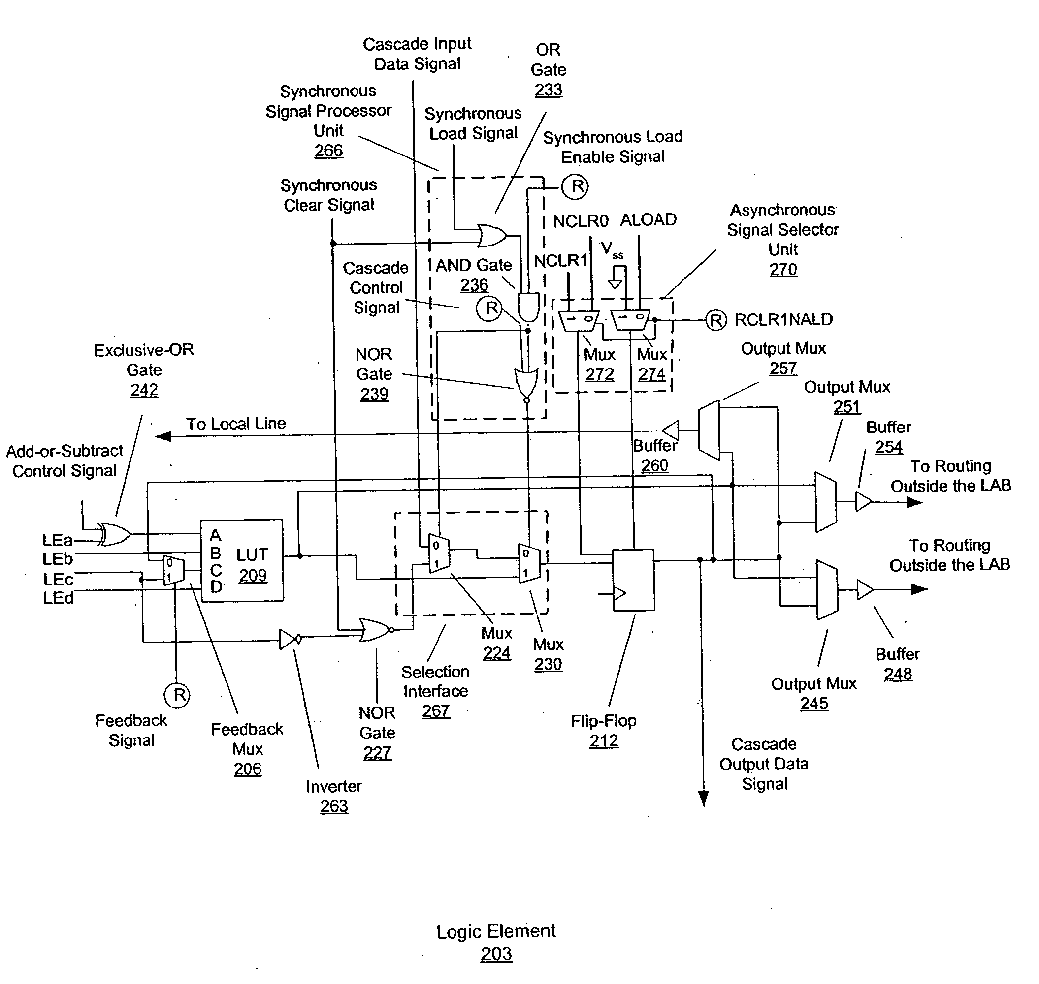
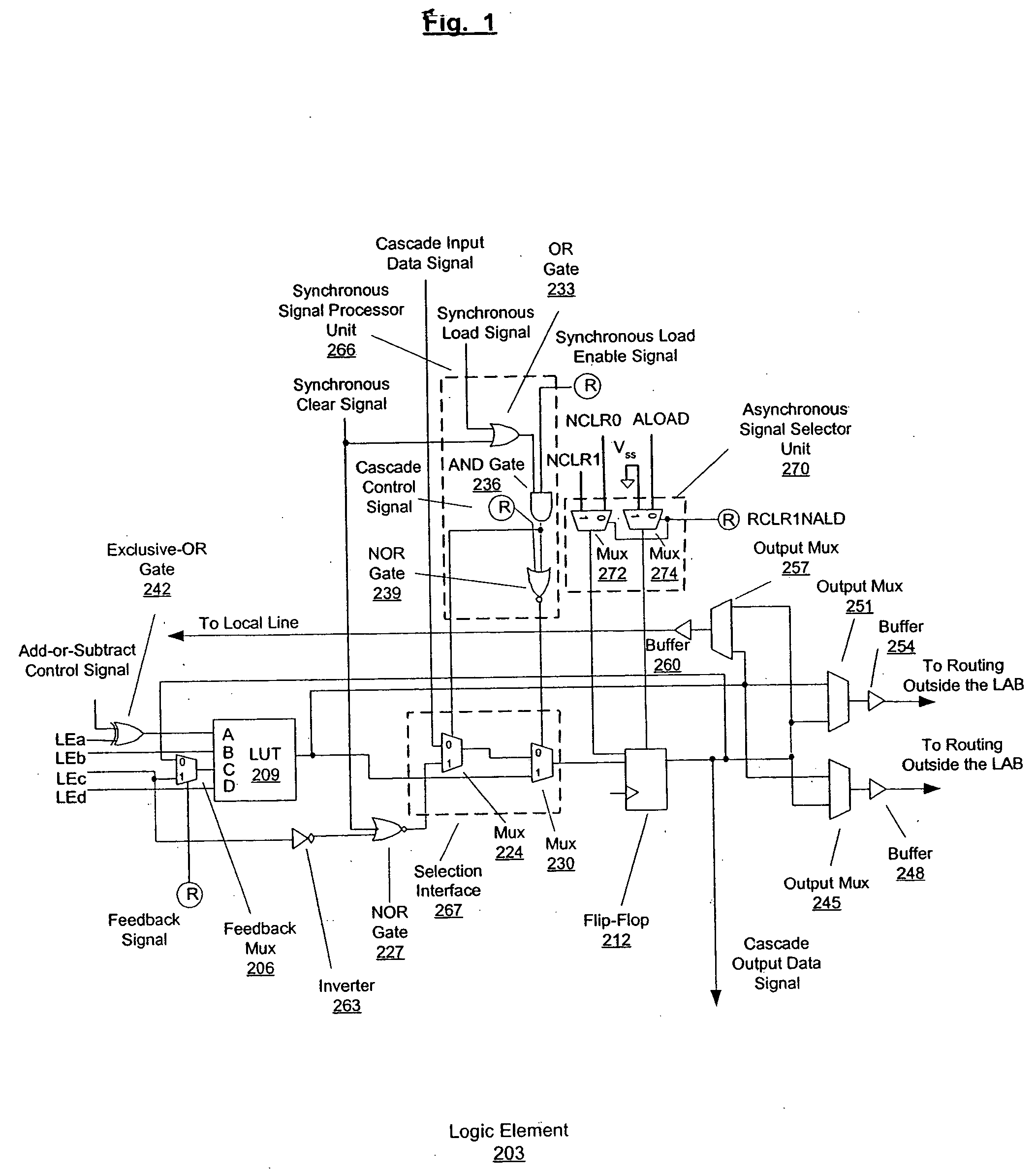
[0026] An embodiment of the invention pertains to programmably connecting the flip-flops and the LUTs within the LE to provide versatile and flexible connections both within the LE and between LEs in the same LAB. Each LEIM selects inputs from a subset of the routing lines within the LAB. The pattern of connections of routing lines to multiplexers is arranged to reduce the need for extra LAB lines by increasing the number of distinct groups of the LAB lines while still maintaining a regular structure that can be readily implemented in an integrated circuit.

[0027]FIG. 1 shows an embodiment of a LE 203 according to the present invention. A first aspect of this embodiment pertains to flexibly coupling a logic function block (e.g., combinational logic such as a LUT 209) and a storage unit (e.g., a register such as a flip-flop 212) within a single LE 203. A selection unit that selects one of its inputs as an output, such as a feedback multiplexer (“mux”) 206, is programmably controlled ...


PUM


Abstract

An embodiment of this invention pertains to a versatile and flexible logic element and logic array block (“LAB”). Each logic element includes a programmable combinational logic function block such as a lookup table (“LUT”) and a flip-flop. Within the logic element, multiplexers are provided to allow the flip-flop and the LUT to be programmably connected such that either the output of the LUT may be connected to the input of the flip-flop or the output of the flip-flop may be connected to the input of the LUT. An additional multiplexer allows the output of the flip-flop in one logic element to be connected to the input of a flip-flop in a different logic element within the same LAB. Output multiplexers selects between the output of the LUT and the output of the flip-flop to generate signals that drive routing lines within the LAB and to routing lines external to the LAB. These output multiplexers are constructed such that the combinational output (output from the LUT) is faster than the output from the flip-flop. A collection of routing lines and multiplexers within the LAB are used to provide inputs to the LUTs. Each of the input multiplexers for each logic element is connected to a subset of the routing lines within the LAB using a specific pattern of connectivity of multiplexers to associated wires that maximizes the efficiency of use of the routing wires. Control signals for the set of logic elements within the LAB are generated using a secondary signal generation unit that minimizes contention for shared signals. One of the control signals is an “add-or-subtract control signal” that allows all of the LEs in a LAB to perform either addition or subtraction under the control of a logic signal. In a PLD supporting redundancy, the carry chain for the LABs is arranged in the same direction that redundancy shifts to remap defective LABs and a multiplexer on the carry input of a LAB is used to select the appropriate carry output from another LAB depending on whether redundancy is engaged.

Description

CROSS-REFERENCE TO RELATED APPLICATIONS [0001] This application is a divisional of U.S. patent application Ser. No. 10 / 280,723 filed on Oct. 24, 2002, the contents of which are incorporated herein by reference in its entirety.STATEMENT REGARDING FEDERALLY SPONSORED RESEARCH OR DEVELOPMENT [0002] Not applicable. REFERENCE TO A COMPACT DISK APPENDIX [0003] Not applicable. BACKGROUND OF THE INVENTION [0004] 1. Field of the Invention [0005] This invention relates generally to a programmable logic device and, in particular, to a programmable logic device having versatile and efficient logic elements and logic array blocks. [0006] 2. Description of the Related Art [0007] A programmable logic device (“PLD”) is a digital, user-configurable integrated circuit used to implement a custom logic function. For the purposes of this description, the term PLD encompasses any digital logic circuit configured by the end-user, and includes a programmable logic array (“PLA”), a field programmable gate a...

Claims


Application Information

Patent Timeline
Patent Type & Authority Applications(United States)
IPC IPC(8): H03K19/173H03K19/177
CPCH03K19/1737H03K19/17764H03K19/17736H03K19/17728H03K19/177
Inventor LEWIS, DAVID M.LEVENTIS, PAULLEE, ANDY L.KIM, HENRYPEDERSEN, BRUCEWYSOCKI, CHRISLANE, CHRISTOPHER F.MARQUARDT, ALEXANDERSANTURKAR, VIKRAMBETZ, VAUGHN
Owner ALTERA CORP
Why Eureka
Try Eureka