Process and structure for repairing defect of liquid crystal display

a liquid crystal display and structure technology, applied in the field of process and structure for repairing defects, can solve the problems of easy splashing of aluminum, easy to occur serious problems such as rc time delay, and possible defects in data or scanning lines by mistake or carelessness, and achieve the effect of efficient shortening a signal transmission lin

Inactive Publication Date: 2005-06-16
HANNSTAR DISPLAY CORPORATION
View PDF2 Cites 9 Cited by
  • Summary
  • Abstract
  • Description
  • Claims
  • Application Information

AI Technical Summary

Benefits of technology

[0014] It is therefore an object of the present invention to propose a process for repairing defects of the liquid crystal display to efficiently shortening a signal transmission line.
[0015] It is therefore another object of the present invention to propose a process for repairing defects of the liquid crystal display to reduce the RC time delay phenomenon.
[0016] It is therefore an additional object of the present invention to propose a process for repairing defects of the liquid crystal display to reduce the moving distance of the laser during repairing.

Problems solved by technology

However, some defects in the data or scanning lines are possible to occur by mistake or through carelessness.
However, due to the low melting point of aluminum, aluminum is easily splashed around when the welding is performed by the laser.
Thus, using the annular repair lines for repairing the defects according to the prior art has the following disadvantages: (1) The signal transmission line is too long after being repaired, so a serious problem of RC time delay is easy to occur; (2) A large area of panel is required to move for performing the repairing action, so the production efficiency will be decreased; and (3) The structure of the repair lines according to the prior art occupies much area of panel, which decreases the utility rate of glass substrates.
(4) The structure of the repair lines according to the prior art easily causes a short circuit, a broken circuit, or a Schottky contact in a contact point.

Method used


Image

  • Process and structure for repairing defect of liquid crystal display
  • Process and structure for repairing defect of liquid crystal display
  • Process and structure for repairing defect of liquid crystal display

Examples


Embodiment Construction

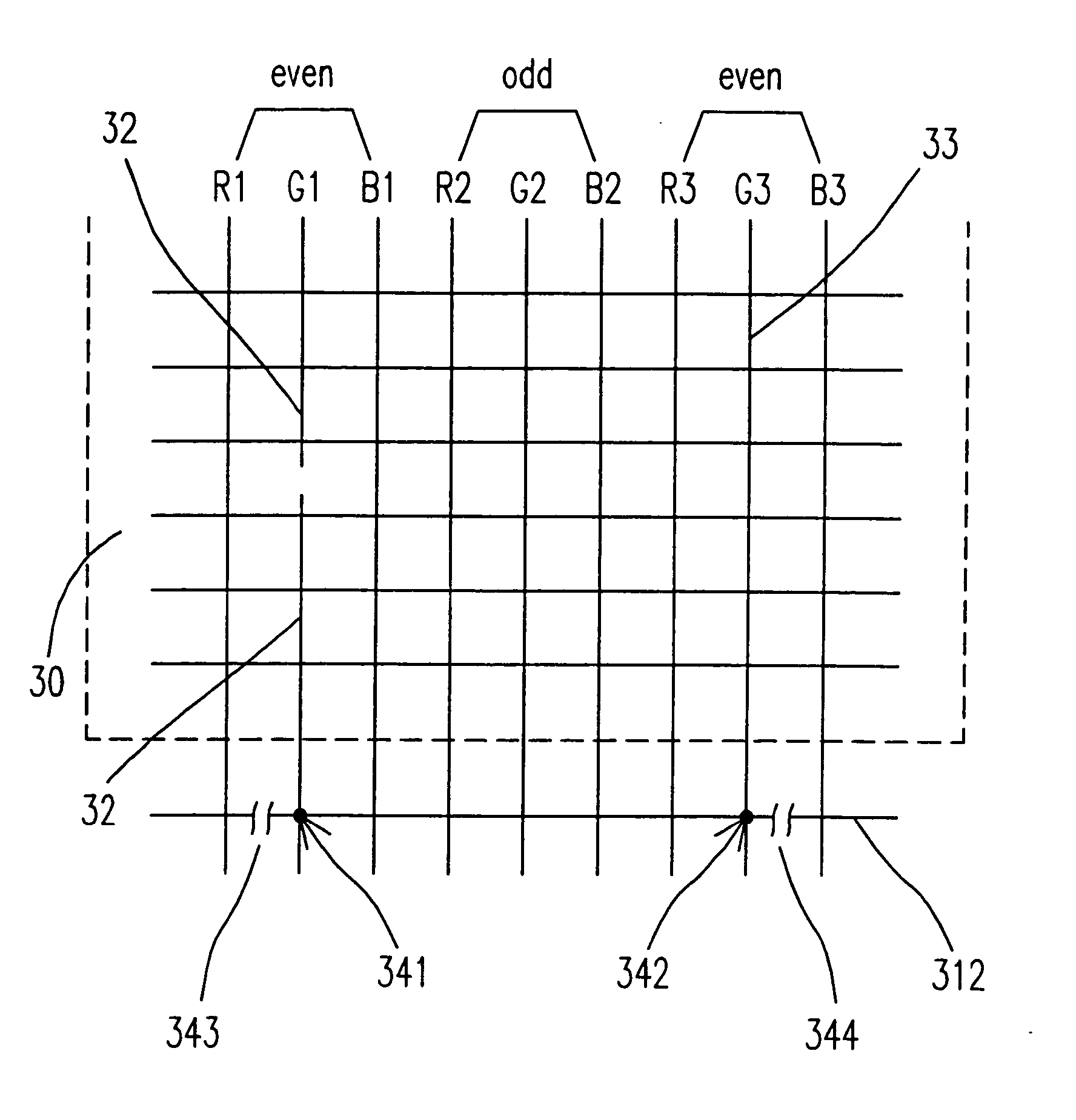
[0044] As shown in FIG. 3A, a rectangle pixel array 30 of the liquid crystal display has a plurality of scanning lines (not shown) and a plurality of data lines (not shown). The present invention provides a repair line 311, 312 located outside of the rectangle pixel array 30, e.g. at one end of the scanning lines or the data lines, for achieving the structure of repairing defects.

[0045] During the typical production of the thin film transistor liquid crystal display, generally the scanning lines are finished by the first photolithography and etching process. However, the data lines are finished by the third or fourth photolithography and etching process. Thus, the defect probability of the scanning line is lower than that of the data line. In addition, if a defect occurred in the scanning line, the scanning line can be re-worked immediately because the process is earlier process.

[0046] The present invention provides a process for repairing defects of a thin film transistor liquid ...


PUM

PropertyMeasurementUnit
wavelengthaaaaaaaaaa
melting pointaaaaaaaaaa

Abstract

A process for repairing defects applied in producing a liquid crystal display, wherein the liquid crystal display includes a pixel array formed by a plurality of scanning lines crossing with a plurality of data lines. The process includes steps of providing an essential repair line located on one side of the pixel array, welding a first intersection point of a defecting data line and the essential repair line and a second intersection point of a normal data line adjacent to the defecting data line and the essential repair line by a first laser to achieve electrical connection, and cutting a first breaking point and a second breaking point of the essential repair line by a second laser to achieve a broken circuit, wherein the first and second intersection points are located two sides of a line segment constructed by the first and second intersection points respectively.

Description

RELATED APPLICATIONS [0001] This application is a divisional of U.S. patent application Ser. No. 09 / 860,945, filed May 17, 2001, entitled: “Process And Structure For Repairing Defect Of Liquid Crystal Display.FIELD OF THE INVENTION [0002] The present invention relates to a process and a structure for repairing defects, and more particularly to a process and a structure for repairing defects of a thin film transistor liquid crystal display (TFTLCD). BACKGROUND OF THE INVENTION [0003] Along with the producing technology development, the liquid crystal display has been become a widely used display device. The working principle of the liquid crystal display is based on the phenomenon that the alignment condition of liquid crystal molecules is changed by applying an electrical field to change the path of light passing through the liquid crystal molecules and the display effect of changing in light and shade is further achieved. [0004]FIG. 1 is a diagram illustrating a unit circuit block ...

Claims


Application Information

Patent Timeline
Patent Type & Authority Applications(United States)
IPC IPC(8): G02F1/1345G02F1/1362
CPCG02F1/1345G02F1/136259G02F2001/13629G02F2001/136263G02F2001/136272G02F1/136286G02F1/136272G02F1/136263G02F1/13629
Inventor HONG, HONG-JYEHSU, GEORGEWANG, CHIH-WEI
Owner HANNSTAR DISPLAY CORPORATION
Why Eureka
Try Eureka