Metal oxide semiconductor (MOS) transistor including a planarized material layer and method of fabricating the same

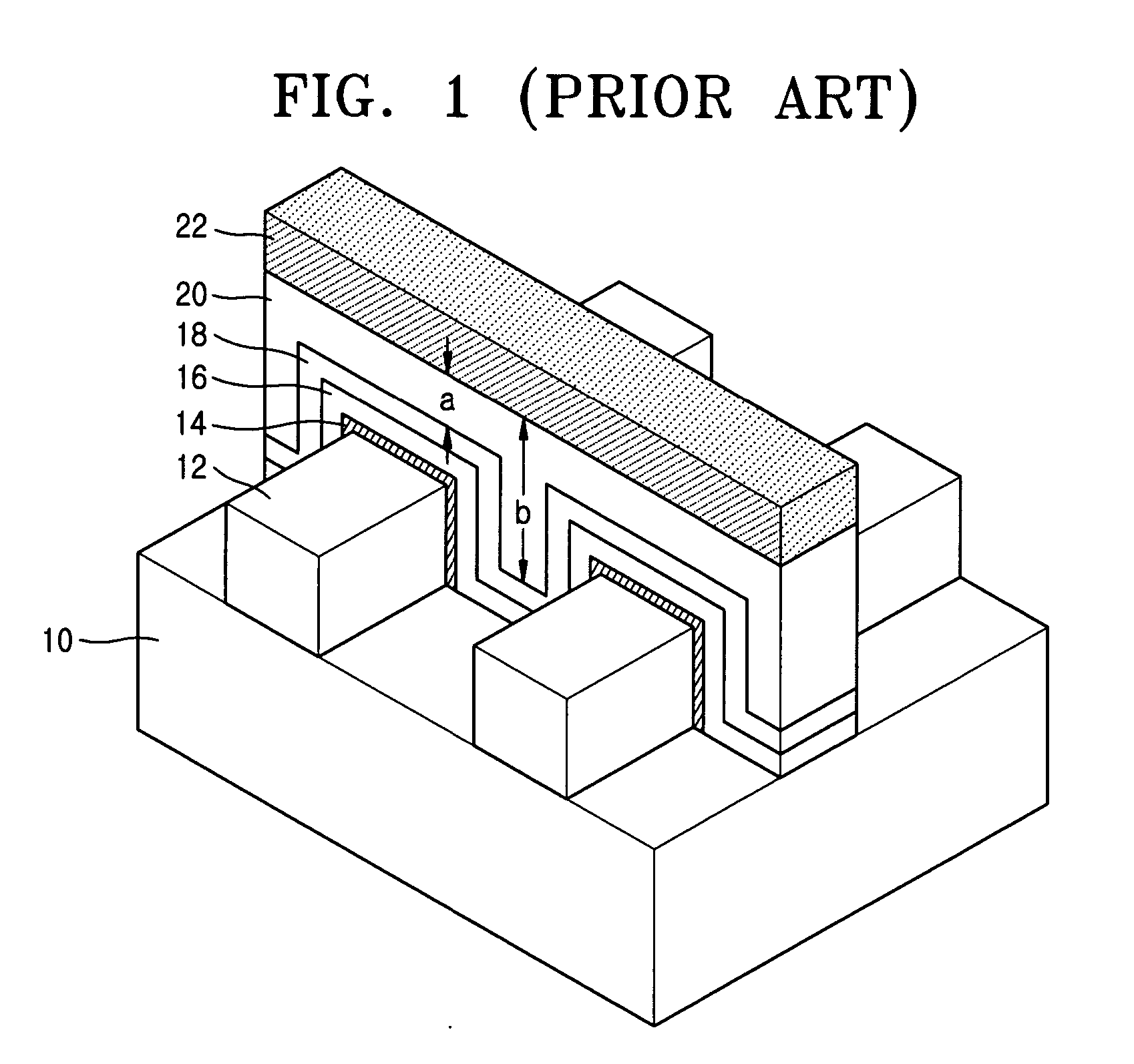
a metal oxide semiconductor and planarized material technology, applied in the field of semiconductor transistors, can solve the problems of imposing limitations on the formation of fine patterns and operation speed, the non-planar layer having a step difference, and the short channel effect is particularly significant, so as to prevent overetching

Inactive Publication Date: 2005-06-16
SAMSUNG ELECTRONICS CO LTD
View PDF7 Cites 6 Cited by
  • Summary
  • Abstract
  • Description
  • Claims
  • Application Information

AI Technical Summary

Benefits of technology

[0011] It is a feature of an embodiment of the present invention to provide a method of fabricating a metal oxide semiconductor (MOS) transistor that is capable of preventing over-etching during formation of a hard mask used to etch a non-planar gate electrode material layer.

Problems solved by technology

A short channel length creates various problems, such as a short channel effect, and imposes limitations on a formation of fine patterns and an operation speed.
The short channel effect is an especially significant problem.
However, such a change in channel structure creates a non-planar layer having a step difference.
Such over-etching damages the photoresist pattern 22 and leads to a poor hard mask profile.
In some cases, notching or breaking occurs in the pattern, thereby leading to the distortion of the hard mask 18.
Furthermore, over-etching excessively recesses the gate electrodes 16 located on the active regions 12 and thus, damages the active regions 12.

Method used


Image

  • Metal oxide semiconductor (MOS) transistor including a planarized material layer and method of fabricating the same
  • Metal oxide semiconductor (MOS) transistor including a planarized material layer and method of fabricating the same
  • Metal oxide semiconductor (MOS) transistor including a planarized material layer and method of fabricating the same

Examples


Embodiment Construction

[0028] Korean Patent Application No. 2003-90942, filed on Dec. 13, 2003, in the Korean Intellectual Property Office, and entitled: “MOS Transistor Using Planarized Material Layer and Method of Fabricating the Same,” is incorporated by reference herein in its entirety.

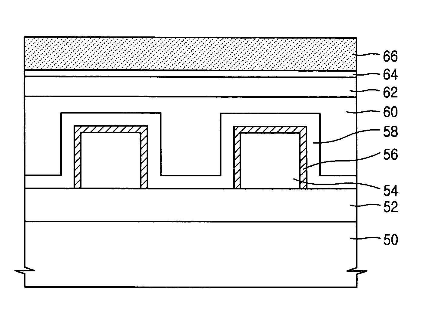
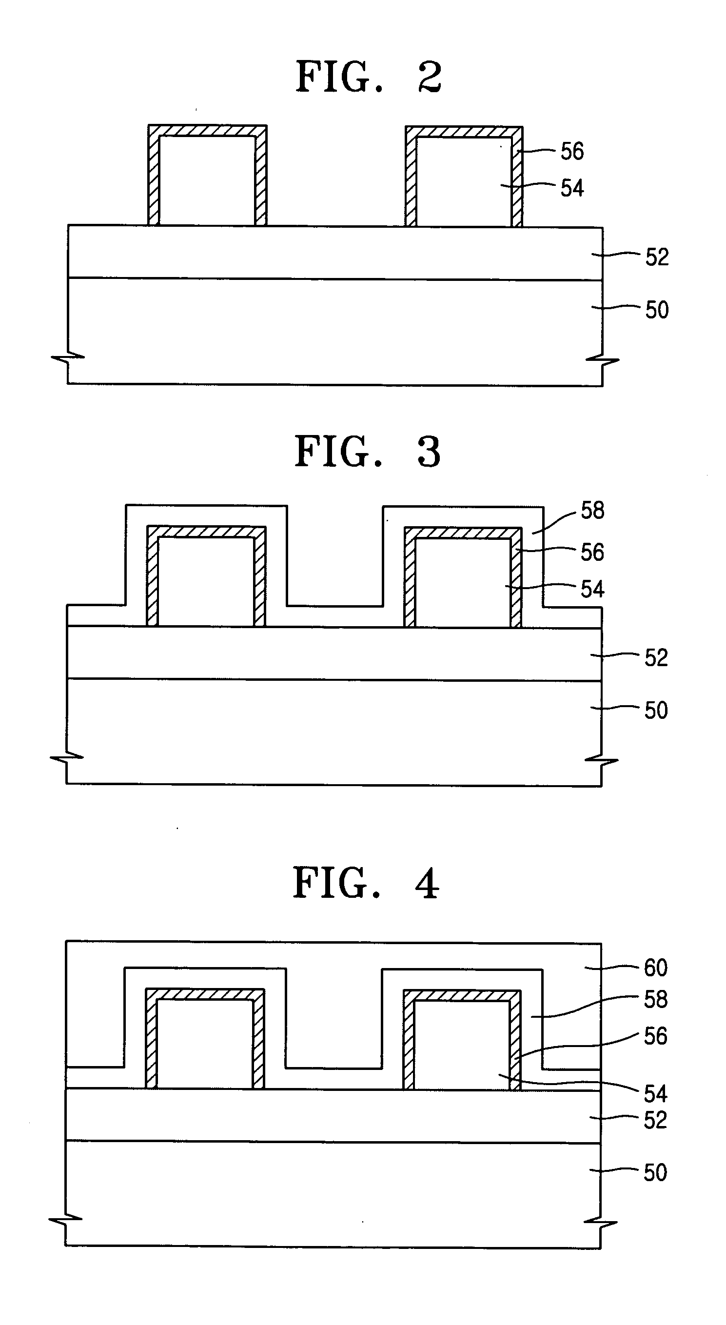
[0029] The present invention will now be described more fully hereinafter with reference to the accompanying drawings, in which exemplary embodiments of the invention are shown. The invention may, however, be embodied in different forms and should not be construed as limited to the embodiments set forth herein. Rather, these embodiments are provided so that this disclosure will be thorough and complete, and will fully convey the scope of the invention to those skilled in the art. In the figures, the dimensions of layers and regions are exaggerated for clarity of illustration. It will also be understood that when a layer is referred to as being “on” another layer or substrate, it can be directly on the other layer or su...


PUM

PropertyMeasurementUnit
temperaturesaaaaaaaaaa
temperatureaaaaaaaaaa

Abstract

A method of fabricating a MOS transistor, and the MOS transistor fabricated by the method, includes providing a substrate, forming a predetermined layer having a non-planar surface on the substrate, the predetermined layer including at least one active region, forming a gate electrode material layer on the non-planar, predetermined layer, forming a material layer and a hard mask layer on an entire surface of the gate electrode material layer, and planarizing a top surface of the material layer to form a planarized material layer, forming a photoresist pattern on the planarized material layer and the hard mask layer to pattern the gate electrode material layer, forming a hard mask pattern by etching the hard mask layer using the photoresist pattern as an etching mask, and forming a predetermined pattern by etching the planarized material layer and the gate electrode material layer according to a shape of the hard mask pattern.

Description

BACKGROUND OF THE INVENTION [0001] 1. Field of the Invention [0002] The present invention relates to a semiconductor transistor and a method of fabricating the same. More particularly, the present invention relates to a metal oxide semiconductor (MOS) transistor including a material layer having a planarized top surface, i.e., a planarized material layer, and a method of fabricating the same. [0003] 2. Description of the Related Art [0004] Due to the increasing integration of semiconductor devices, lengths of gate channels are decreasing. A short channel length creates various problems, such as a short channel effect, and imposes limitations on a formation of fine patterns and an operation speed. The short channel effect is an especially significant problem. For example, an increase in a field near a drain region creates a punch-through, in which a drain depletion region penetrates a potential barrier around a source region. Resultantly, thermions create an avalanche and a perpendic...

Claims


Application Information

Patent Timeline
Patent Type & Authority Applications(United States)
IPC IPC(8): H01L21/00H01L21/336H01L21/84H01L21/335H01L27/12H01L29/786
CPCH01L21/84H01L29/785H01L29/66795H01L27/1203H01L21/18
Inventor KIM, JIN-YOUNGSHIGENOBU, MAEDAKANG, CHANG-JINYANG, JEONG-HWAN
Owner SAMSUNG ELECTRONICS CO LTD
Why Eureka
Try Eureka