Thin film transistor liquid crystal display and fabrication method thereof

a technology of thin film transistors and liquid crystal displays, applied in the direction of optics, semiconductor devices, instruments, etc., can solve the problems of increasing costs and lowering throughput, and achieve the effect of reducing the number of required photolithography steps

Active Publication Date: 2005-02-17
AU OPTRONICS CORP
View PDF3 Cites 5 Cited by
  • Summary
  • Abstract
  • Description
  • Claims
  • Application Information

AI Technical Summary

Benefits of technology

[0015] Accordingly, an object of the present invention is to reduce the number of required photolithography steps in production of a TFT-LCD.

Problems solved by technology

Owing to the two steps of contact-hole manufacture, up to six photolithography steps are required, lowering throughput, and increasing costs.

Method used


Image

  • Thin film transistor liquid crystal display and fabrication method thereof
  • Thin film transistor liquid crystal display and fabrication method thereof
  • Thin film transistor liquid crystal display and fabrication method thereof

Examples


Embodiment Construction

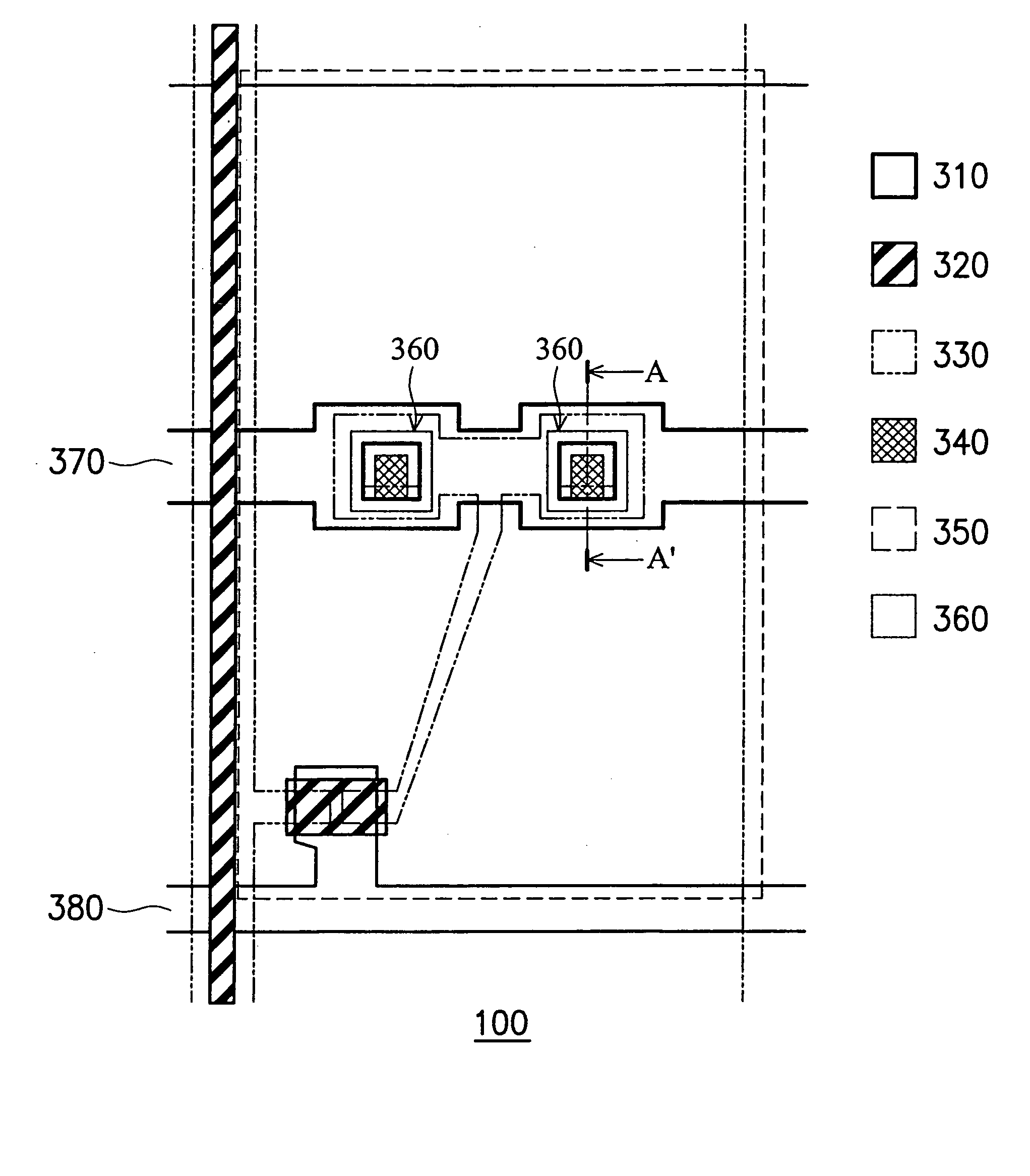
[0024]FIG. 3 is a top view showing a TFT-LCD in the invention. The TFT-LCD comprises a transparent substrate 100, gate line area 310, n+ doped a-Si layer 320, source / drain electrode area 330, contact-hole area 340, indium tin oxide layer 350, light shielding matrix (black matrix) 360 on a color filter, capacitor line 370, and gate line 380.

[0025]FIGS. 4A-4E are cross-sections of the TFT-LCD taken at the line A-A′ in FIG. 3, showing the manufacturing process of TFT-LCD in the invention.

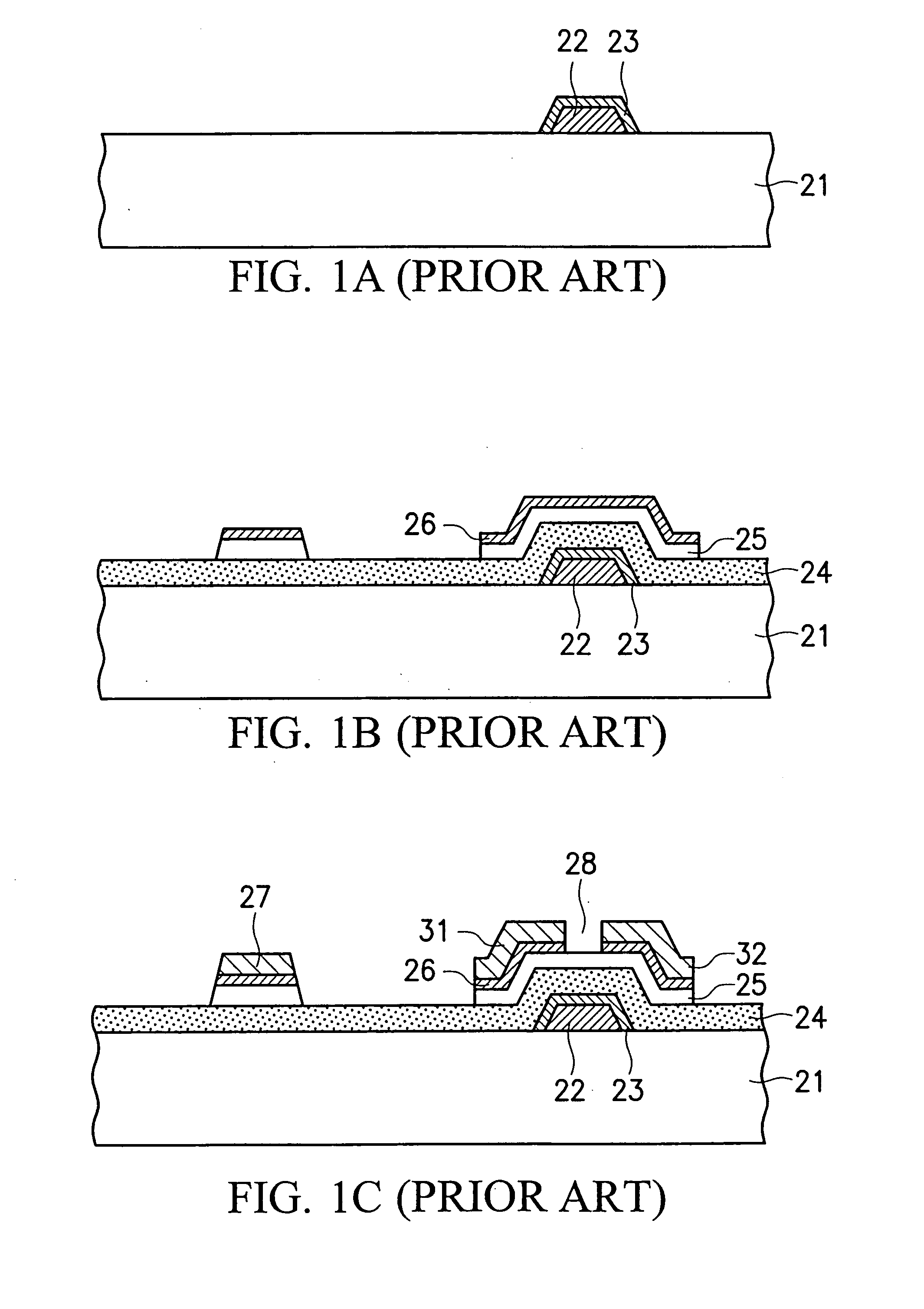
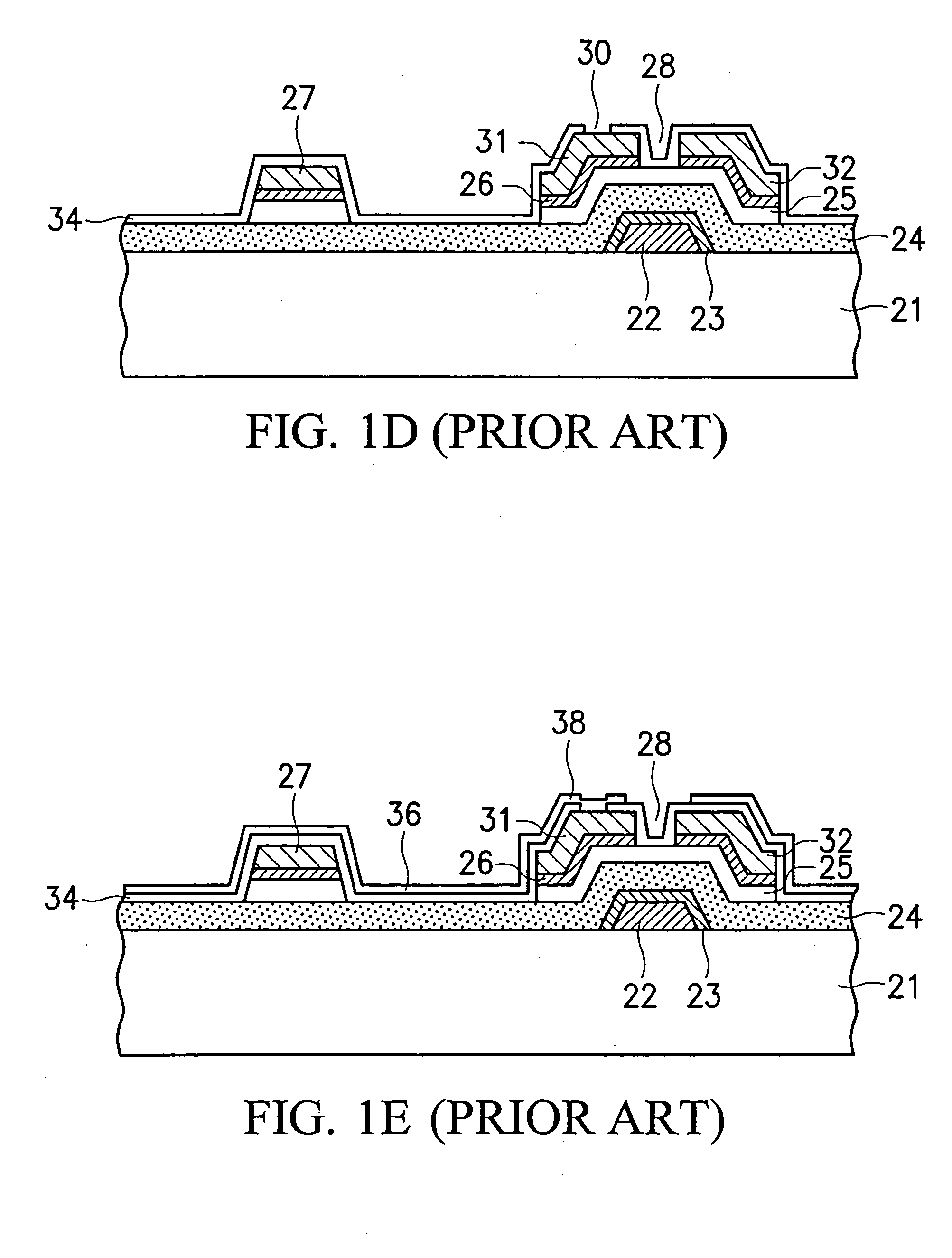
[0026] First, as in FIG. 4A, a first metal layer of, for example, Mo-Al-Nd alloy is deposited on a transparent substrate 100, and then defined by a first photolithography step to form gate electrodes 102.

[0027] Next, as in FIG. 4B, a gate insulating layer 104 is formed on the gate electrodes 102. For example, an oxide layer is formed on the gate electrodes 102 by chemical vapor deposition (CVD). Next, a semiconductor layer (not shown) of, for example, n+ doped a-Si is formed on the gate insulating l...


PUM

PropertyMeasurementUnit
transparentaaaaaaaaaa
transparent conductiveaaaaaaaaaa
shapeaaaaaaaaaa

Abstract

A thin film transistor liquid crystal display (TFT-LCD) and fabrication method thereof. The fabrication method includes depositing a first metal layer on a transparent substrate, patterning the first metal layer to form at least two adjacent gate electrodes, forming a gate insulating layer on the gate electrodes, forming a semiconductor layer on the insulating layer, patterning the semiconductor layer into a predetermined shape, depositing a second metal layer on the transparent substrate, patterning the second metal layer to form a source/drain electrode layer, and depositing an insulating layer on the transparent substrate. A contact hole is defined via the insulating layer, source/drain electrode layer, and gate insulating layer, exposing a part of the surface of transparent substrate between the adjacent gate electrodes. A transparent conductive layer is deposited on the transparent substrate, and a light-shielding matrix is formed directly above the contact hole.

Description

BACKGROUND OF THE INVENTION [0001] 1. Field of the Invention [0002] The present invention relates to a thin film transistor liquid crystal display (TFT-LCD), and more particularly to a TFT-LCD manufacturing process with fewer photolithography steps. [0003] 2. Description of the Related Art [0004] Liquid crystal display (LCD) is a commonly used flat panel display technology. Owing to dielectric anisotropy and conductive anisotropy of liquid crystal molecules, molecular orientation of liquid crystals can be shifted under an external electronic field, such that various optical effects are produced. [0005] An LCD panel is generally made up of two substrates, with a certain gap preserved therebetween, and a liquid crystal layer filled in the gap. Respective electrodes are formed on the two substrates, respectively, to control the orientation and shift of liquid crystal molecules. [0006] A TFT-LCD panel is generally made up of a TFT array substrate and a color filter substrate. The detail...

Claims


Application Information

Patent Timeline
Patent Type & Authority Applications(United States)
IPC IPC(8): G02F1/1335G02F1/1343G02F1/1362H01L21/00H01L21/84H01L29/04H01L29/76H01L31/036H01L31/0376
CPCG02F1/136227G02F1/133512
Inventor CHEN, MAW-SONG
Owner AU OPTRONICS CORP
Why Eureka
Try Eureka