Semiconductor readout circuit

Inactive Publication Date: 2005-06-23
SHARP KK
View PDF7 Cites 0 Cited by
  • Summary
  • Abstract
  • Description
  • Claims
  • Application Information

AI Technical Summary

Benefits of technology

[0013] More specifically, in the semiconductor readout circuit with the second feature, the potential difference detecting circuit is designed to reduce the output voltage when the potential of the corresponding data line is higher than the potential of the reference data line. Also, in the semiconductor readout circuit with the second feature, the fixed potential is a ground potential, and the current control circuit includes a P-type MOSFET that receives the output of the potential difference detecting circuit as a gate input. When the potential of the corresponding data line is higher than the potential of the reference data line in this structure, the output voltage at the potential difference detecting circuit decreases. As a result of this, the amount of current flowing in the P-type MOSFET of the current control circuit increases, and the potential of the corresponding data line decreases and approaches the ground potential. On the other hand, when the potential of the corresponding data line is lower than the potential of the reference data line, the output voltage at the potential difference detecting circuit increases. As a result of this, the amount of current flowing in the P-type MOSFET of the current control circuit decreases, and the potential of the corresponding data line is prevented from decreasing. Therefore, the current control circuit functions to make the potential of the corresponding data line substantially equal to the potential of the reference data line. Accordingly, the corresponding data line is indirectly equalized to the reference data line, and the effects of the semiconductor readout circuit with the first feature can be achieved.
[0014] Also in the semiconductor readout circuit with the second feature, the potential difference detecting circuit is designed to increase the output voltage when the potential of the corresponding data line is higher than the potential of the reference data line. Further, the fixed potential is a ground potential, and the current control circuit includes an N-type MOSFET that receives the output of the potential difference detecting circuit as a gate input and is located between the corresponding data line and the fixed potential line. When the potential of the corresponding data line is higher than the potential of the reference data line in this structure, the output voltage at the potential difference detecting circuit increases. As a result of this, the amount of current flowing in the N-type MOSFET of the current control circuit increases, and the potential of the corresponding data line decreases and approaches the ground potential. On the other hand, when the potential of the corresponding data line is lower than the potential of the reference data line, the output voltage at the potential difference detecting circuit decreases. As a result of this, the amount of current flowing in the N-type MOSFET of the current control circuit decreases, and the potential of the corresponding data line is prevented from decreasing. Therefore, the current control circuit functions to make the potential of the corresponding data line substantially equal to the potential of the reference data line. Accordingly, the corresponding data line is indirectly equalized to the reference data line, and the effects of the semiconductor readout circuit with the first feature can be achieved.
[0015] Also in the semiconductor readout circuit with the second feature, the potential difference detecting circuit is designed to reduce the output voltage when the potential of the corresponding data line is higher than the potential of the reference data line. Further, the fixed potential is a source potential, and the current control circuit includes an N-type MOSFET that receives the output of the potential difference detecting circuit as a gate input and is located between the corresponding data line and the fixed potential line. When the potential of the corresponding data line is lower than the potential of the reference data line in this structure, the output voltage at the potential difference detecting circuit increases. As a result of this, the amount of current flowing in th

Problems solved by technology

However, there are the following problems with the above conventional data readout method.
This leads to an increase in chip area.
If a problem is caused in one of the data lines during the process in such a structure, the voltages at all the data lines DL become unstable, and

Method used


Image

  • Semiconductor readout circuit
  • Semiconductor readout circuit
  • Semiconductor readout circuit

Examples


Example

First Embodiment

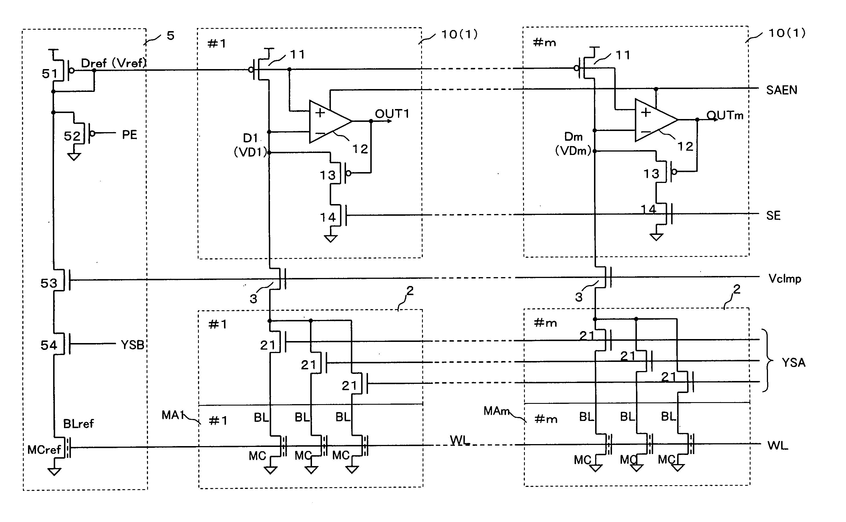
[0028]FIG. 1 is a circuit diagram illustrating the structure of the inventive circuit 10. In this embodiment, a semiconductor device that includes plural memory arrays MA1 through MAm is used. In each of the memory arrays MA1 through MAm, a memory cell MC is selected according to an address signal that is input to the semiconductor device from the outside or is generated inside the semiconductor device. The data stored in the selected memory cells appear as a minute potential change on data lines D1 through Dm that are provided for the respective memory arrays MA1 through MA1. The potential of each of the data lines D1 through Dm is compared with the potential of a common reference data line Dref, and the potential difference is amplified. One set of data are then read out from each of the memory arrays MA1 through MA1.

[0029] This embodiment is described on the assumption that the inventive circuit 1 is a flash-memory readout circuit. Therefore, flash memory cells ...

Example

[0042] Next, other embodiments (second through fourth embodiments) of the inventive circuit 1 are described.

Example

[0043] In each inventive circuit 10 of the first embodiment 1, a series circuit formed by the PMOS 13 and the NMOS 14 is interposed between the data line Di and the ground line to form a current control circuit that controls the amount of current flowing from the data line Di to the ground line, according to the potential of the output OUTi that is the output as to the detected potential difference between the potential VDi of the data line Di and the reference potential Vref. In each inventive circuit 20 of the second embodiment, on the other hand, the PMOS 13 is replaced with an NMOS 23, so that the polarities of the differential inputs to the sense amplifier 12 are reversed as shown in FIG. 3. Thus, the same equalizing function as that of the first embodiment can be obtained. The other components and aspects of each inventive circuit 20 of the second embodiment are the same as those of the first embodiment, and therefore, explanation of them is omitted herein.


PUM


Abstract

A semiconductor readout circuit reads out a potential of each of plural data lines by comparing the potential with a potential of a common reference data line, using a sense amplifier provided for each of the data lines. This semiconductor readout circuit has a current control circuit provided for each of the data lines. The current control circuit controls the potential of the corresponding one of the data lines so that a potential difference between the potential of the corresponding data line and the potential of the reference data line can be reduced based on an output as to the potential difference detected by the sense amplifier.

Description

CROSS REFERENCE TO RELATED APPLICATIONS [0001] This Nonprovisional application claims priority under 35 U.S.C. § 119 (a) on Patent Application No. 2003-419757 filed in Japan on 17 Dec. 2003, the entire contents of which are hereby incorporated by reference. BACKGROUND OF THE INVENTION [0002] 1. Field of the Invention [0003] The present invention relates to a data readout circuit for semiconductor devices. [0004] 2. Description of the Related Art [0005] JP-A 10-11974 (1998) discloses a circuit that amplifies data accumulated in a memory cell in a semiconductor device before reading the data out (see FIG. 7). In this circuit structure, drivers that have higher ability than the current driving ability of the pull-ups and the memory cells of data lines DL and DLB are provided for the respective data lines DL and DLB. With the drivers, the potentials of the data lines DL and DLB become equal to one another in the initial stage of a data readout operation (i.e., during the process of equa...

Claims


Application Information

Patent Timeline
IPC IPC(8): G11C11/419G11C7/02G11C7/06G11C7/08G11C7/10G11C7/12G11C16/06
CPCG11C7/062G11C7/12G11C7/1069G11C7/1051G11C7/1063
Inventor ITO, NOBUHIKOYAMAMOTO, KAORUYAMAUCHI, YOSHIMITSU
Owner SHARP KK
Why Eureka
Try Eureka