System and method for improving solder joint reliability in an integrated circuit package

a technology of integrated circuit and reliability, which is applied in the direction of printed circuit aspects, sustainable manufacturing/processing, final product manufacturing, etc., can solve the problems of qfn integrated circuit package becoming electrically (and even physically) disconnected from the underlying printed circuit board, solder joint cracking, solder material delaminate, etc., to improve solder joint reliability, increase the strength of a solder bond, and increase the reliability of the solder join

Active Publication Date: 2005-06-30
STMICROELECTRONICS SRL
View PDF8 Cites 20 Cited by
  • Summary
  • Abstract
  • Description
  • Claims
  • Application Information

AI Technical Summary

Benefits of technology

[0011] When the QFN integrated circuit package is soldered to an underlying printed circuit board then solder is applied to the external bottom surface of the die pad and to the terminals. The applied solder also fills the solder slots in the external bottom surface of the die pad and also fills the solder slots in the terminals. The remaining areas (i.e., the areas not having solder slots) will also be coated by solder after the solder reflow process. The solder that fills the solder slots strengthens the solder bond against the lateral forces that the solder bond may experience. In this manner the solder within the solder slots increases the solder joint reliability of the QFN integrated circuit package.
[0012] It is an object of the present invention to provide an improved system and method for improving solder joint reliability in a QFN integrated circuit package.
[0013] It is also an object of the present invention to provide an improved system and method for increasing the strength of a solder bond between a QFN integrated circuit package and an underlying printed circuit board.

Problems solved by technology

If the stress on the solder joint reaches sufficiently high levels then the solder joint may crack and the solder material may delaminate.
This may cause the QFN integrated circuit package to become electrically (and even physically) disconnected from the underlying printed circuit board.

Method used


Image

  • System and method for improving solder joint reliability in an integrated circuit package
  • System and method for improving solder joint reliability in an integrated circuit package
  • System and method for improving solder joint reliability in an integrated circuit package

Examples


Embodiment Construction

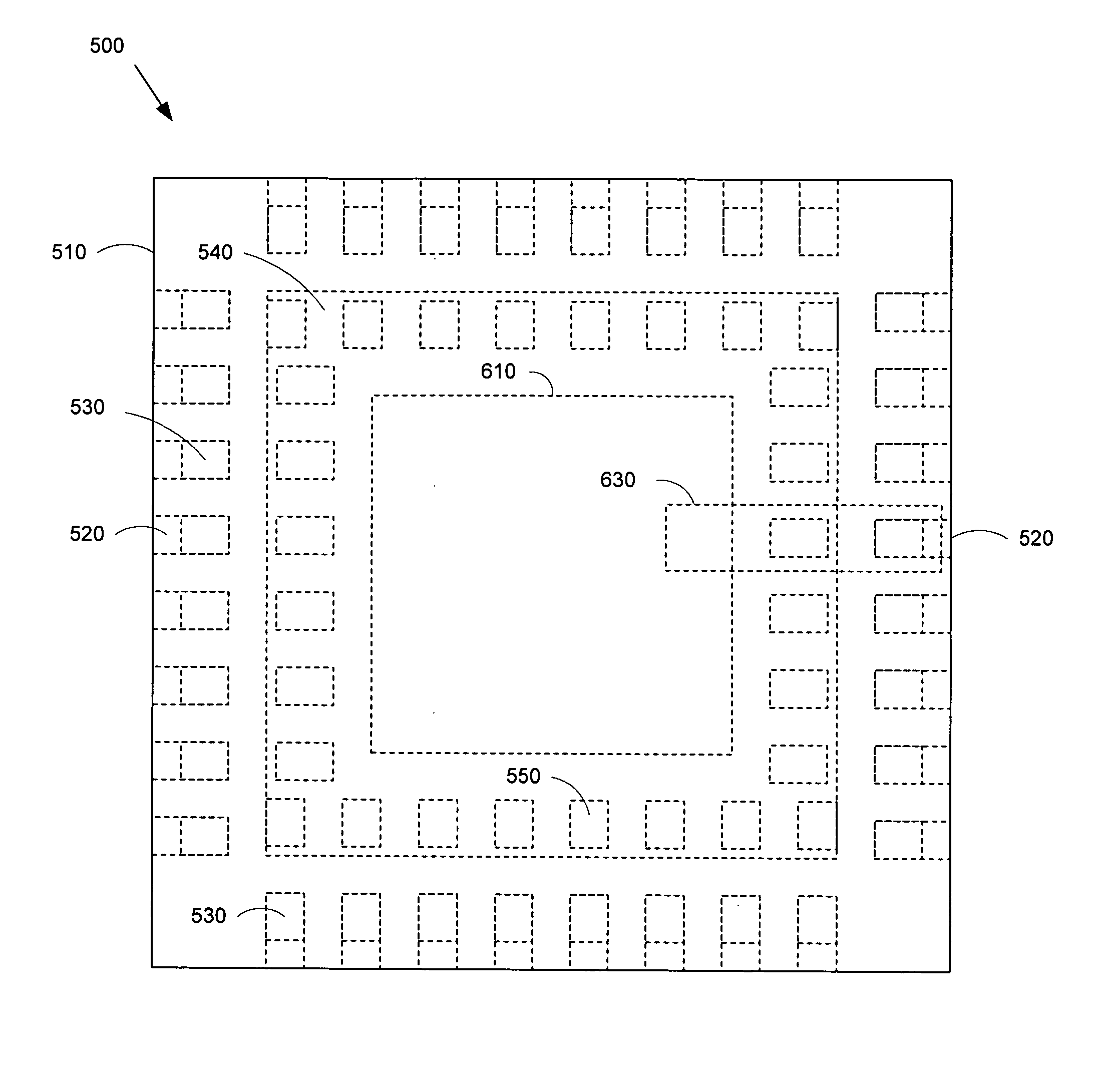
[0030]FIGS. 1 through 11, discussed below, and the various embodiments used to describe the principles of the present invention in this patent document are by way of illustration only and should not be construed in any way to limit the scope of the invention. Those skilled in the art will understand that the principles of the present invention may be implemented in any suitably arranged QFN integrated circuit package.

[0031] In particular, the apparatus and method of the present invention will be described for an integrated circuit package that has terminals on four (4) sides. It is understood that the integrated circuit package with four (4) sides is merely an example and that the apparatus and method of the invention may be applied to any number of sides (e.g., one, two, three, or four) of an integrated circuit package.

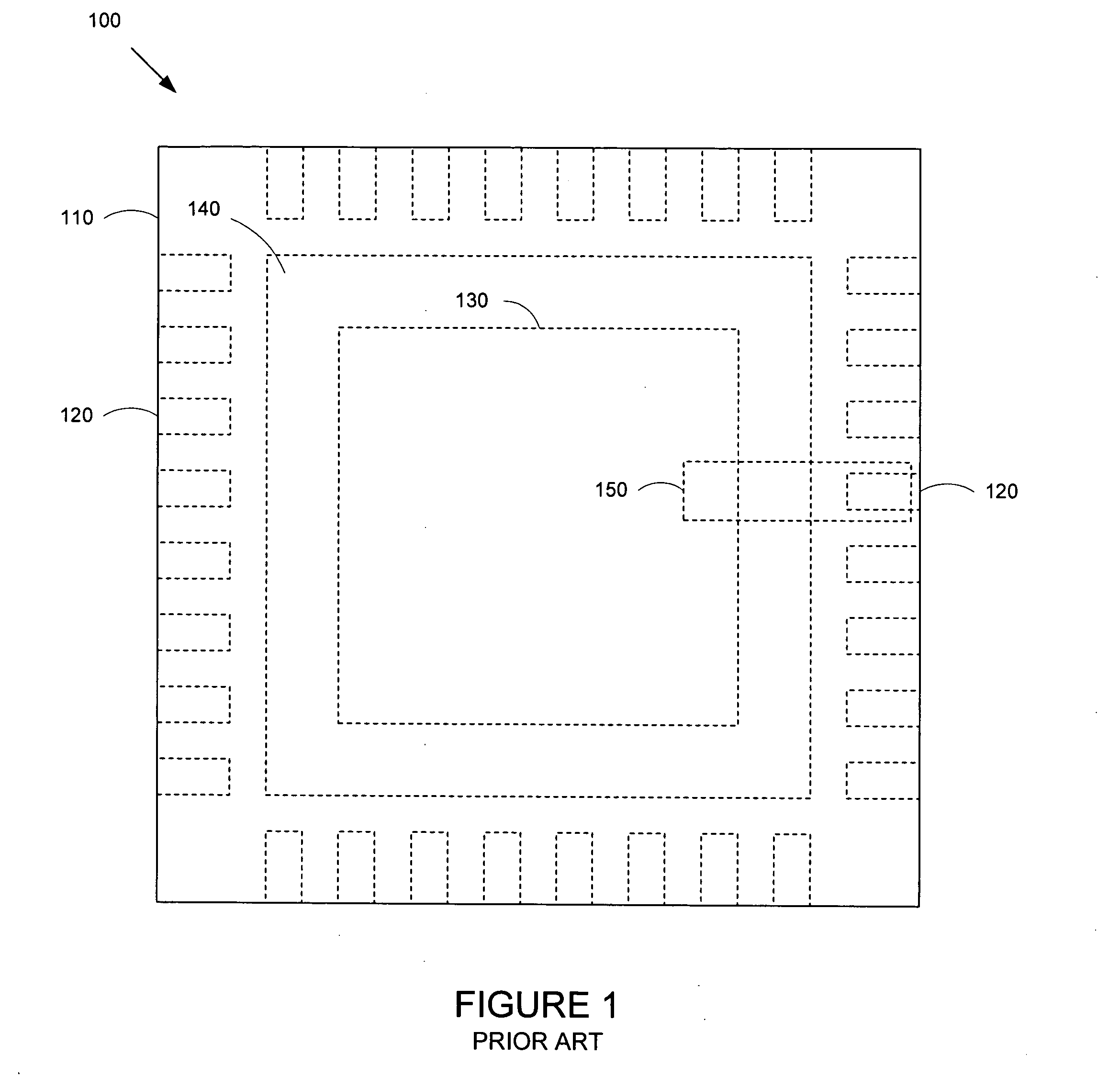
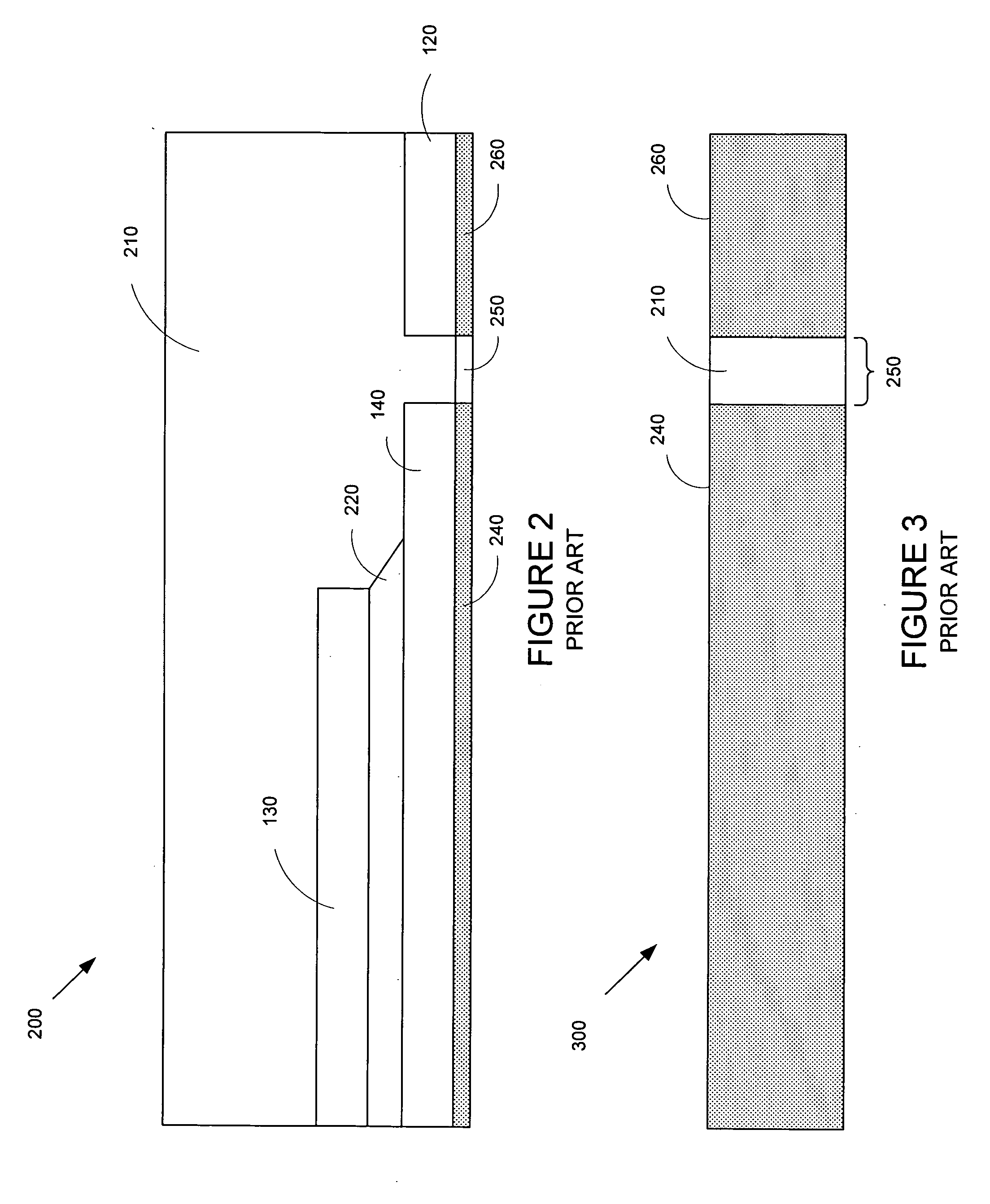
[0032]FIG. 1 illustrates a top view of an exemplary prior art QFN (quad, flat, non-leaded) integrated circuit package 100. QFN integrated circuit package 100 compr...


PUM


Abstract

A system and method is disclosed for improving solder joint reliability in an integrated circuit package. Each terminal of a quad, flat, non-leaded integrated circuit package is formed having portions that define a solder slot in the bottom surface of the terminal. An external surface of the die pad of the integrated circuit package is also formed having portions that define a plurality of solder slots on the periphery of the die pad. When solder is applied to the die pad and to the terminals, the solder that fills the solder slots increases the solder joint reliability of the integrated circuit package.

Description

TECHNICAL FIELD OF THE INVENTION [0001] The present invention is directed, in general, to integrated circuit packages and, more specifically, to a system and method for improving solder joint reliability in an integrated circuit package. BACKGROUND OF THE INVENTION [0002] New types of integrated circuits are continually being developed. Some of the newer integrated circuit devices have an increased number of functions and operate at higher speeds than older types of integrated circuits. The newer types of integrated circuits often produce more heat and operate at higher device temperatures than older types of integrated circuits. [0003] The semiconductor industry has been developing newer types of integrated circuit packages for providing efficient and cost effective heat removal for such integrated circuits. The design goal is to make plastic integrated circuit packages that are smaller, thinner, cooler, cheaper, and easy and quick to manufacture. [0004] One of the newer types of i...

Claims


Application Information

Patent Timeline
Patent Type & Authority Applications(United States)
IPC IPC(8): H01L23/50H01L23/31H01L23/495H05K3/34
CPCH01L23/3107H01L23/49548H01L23/49582H05K3/341H05K3/3442H05K2201/0373H01L2224/32245H05K2201/10727H05K2201/10969H01L2924/00014H05K2201/09745H01L21/4821H01L2224/45099Y02P70/50
Inventor CHIU, ANTHONY M.TEE, TONG YAN
Owner STMICROELECTRONICS SRL
Why Eureka
Try Eureka