Ball grid array package having improved reliability and method of manufacturing the same

a grid array and reliability technology, applied in printed circuits, non-metallic protective coating applications, dielectric characteristics, etc., can solve the problems of deformation of the solder joint reliability (sjr) of the resulting device, and achieve the reduction or prevention of improved solder joint reliability (sjr), and reduced deformation of the conductive ball lands

Inactive Publication Date: 2006-07-04
SAMSUNG ELECTRONICS CO LTD
View PDF11 Cites 10 Cited by
  • Summary
  • Abstract
  • Description
  • Claims
  • Application Information

AI Technical Summary

Benefits of technology

[0008]The present invention provides exemplary embodiments of ball grid array (BGA) packages in which the deformation of the conductive ball lands is reduced or prevented and which will tend to exhibit improved solder joint reliability (SJR) as a result. The present invention also provides exemplary methods for manufacturing BGA packages in which the deformation of the conductive ball lands may be reduced.

Problems solved by technology

Overtime, these shearing stresses tend to degrade the solder joint reliability (SJR) of the resulting device.

Method used


Image

  • Ball grid array package having improved reliability and method of manufacturing the same
  • Ball grid array package having improved reliability and method of manufacturing the same
  • Ball grid array package having improved reliability and method of manufacturing the same

Examples


Embodiment Construction

[0018]The present invention will now be described more fully with reference to the accompanying drawings, in which certain exemplary embodiments of the invention are shown. Those of ordinary skill in the art will, however, appreciate that the present invention may be embodied in many different forms and should therefore not be construed as being limited to the particular exemplary embodiments described and illustrated herein. These exemplary embodiments are provided, however, so that the present disclosure will be thorough and complete and will fully convey the concept of the invention to those of ordinary skill in the art.

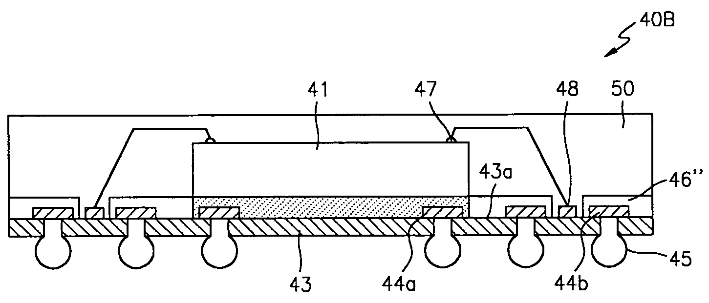
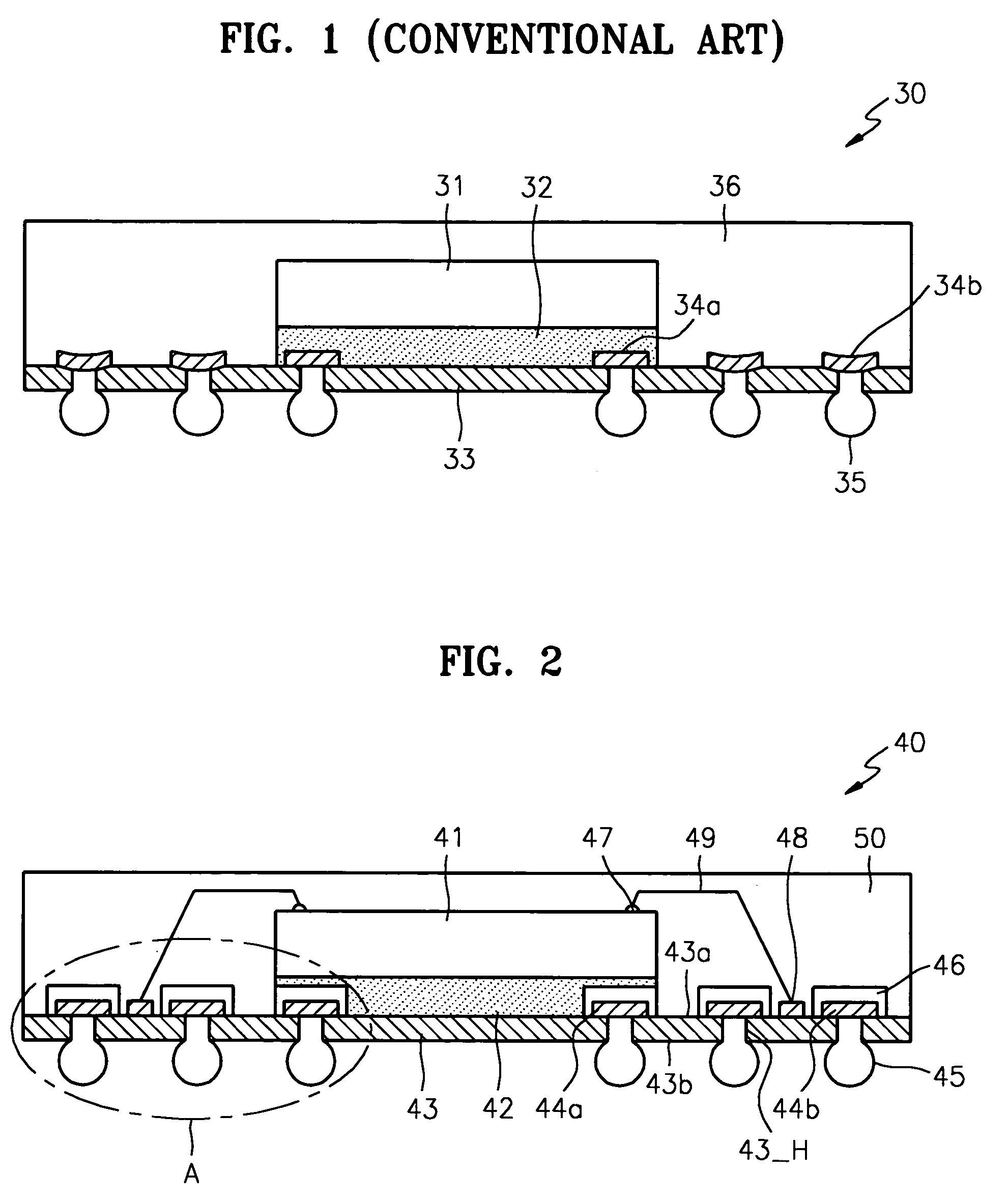
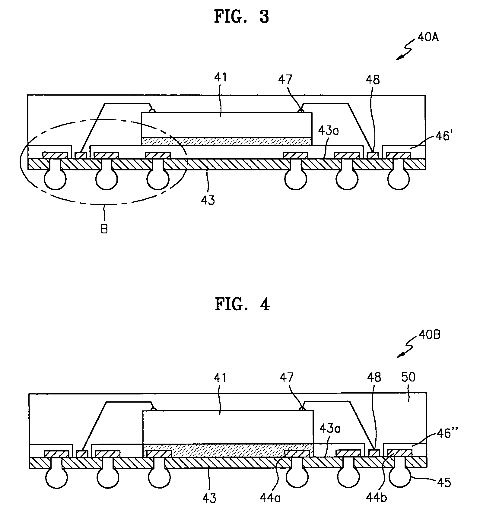
[0019]FIG. 2 is a cross-sectional view of a BGA package 40 according to a first exemplary embodiment of the present invention. As shown in FIG. 2, bond fingers 48 and conductive ball lands 44a and 44b are formed on a top surface 43a of an substrate 43 formed from an insulating material. A variety of insulating materials may be used singly or in combination to form...


PUM


Abstract

A ball grid array package utilizing a layer of an elastic insulating material to protect conductive ball lands from deformation during subsequent processing and use of the resulting device and a method of manufacturing the same are disclosed. The elastic insulating layer preferably has a modulus of elasticity no greater than about 20 MPa or less to absorb and or distribute mechanical stress applied to conductive ball lands directly or through solder ball joints or other structures and thereby improve the solder joint reliability (SJR) of the resulting device.

Description

CROSS-REFERENCE TO RELATED APPLICATIONS[0001]This application claims the priority of Korean Patent Application No. 2003-5935, filed on Jan. 29, 2003, in the Korean Intellectual Property Office, the disclosure of which is incorporated herein in its entirety by reference.BACKGROUND OF THE INVENTION[0002]1. Field of the Invention[0003]The present invention relates to semiconductor packages and methods of manufacturing semiconductor packages and, more particularly, relates to a ball grid array (BGA) package and a method of manufacturing such a package.[0004]2. Description of the Related Art[0005]Ball grid array (BGA) packages are used for mounting of and making electrical connections to semiconductor chips. FIG. 1 is a cross-sectional view of a conventional BGA package 30. As illustrated in FIG. 1, the BGA package 30 includes a semiconductor chip 31 mounted on a top surface of a substrate 33 via an adhesive 32. The exposed top surfaces of the semiconductor chip 31 and the substrate 33 a...

Claims


Application Information

Patent Timeline
Patent Type & Authority Patents(United States)
IPC IPC(8): H01L21/44H01L21/48H01L21/50H01L23/48H01L23/498H05K1/02H05K1/11H05K3/28H05K3/34
CPCH05K1/0271H01L23/49816H01L24/32H01L24/48H01L2924/01047H01L2924/01059H01L2924/01078H01L2924/01079H01L2924/014H01L2924/15311H05K1/112H05K3/28H05K3/3457H05K2201/0133H05K2201/0394H05K2201/09472H01L2224/05599H01L2224/131H01L2224/32057H01L2224/32225H01L2224/48095H01L2224/48227H01L2224/48228H01L2224/48465H01L2224/73265H01L2224/83385H01L2224/85399H01L2224/92247H01L2924/01005H01L2924/01006H01L2924/01028H01L2924/01029H01L2924/00014H01L2924/01033H01L2224/0401H01L2224/45099H01L2924/00H01L2924/3512H01L2924/181H01L2924/00012H01L23/48
Inventor SEO, JEONG-WOO
Owner SAMSUNG ELECTRONICS CO LTD
Why Eureka
Try Eureka