Board structure, a ball grid array (BGA) package and method thereof, and a solder ball and method thereof

a technology of grid array and solder ball, which is applied in the direction of printed circuit aspects, sustainable manufacturing/processing, final product manufacturing, etc., can solve the problems of solder ball cracks, solder ball detachment or failure to attach to the printed circuit board, etc., to suppress the coming off of solder ball and increase the reliability of solder ball

Inactive Publication Date: 2007-05-10
SAMSUNG ELECTRONICS CO LTD
View PDF34 Cites 9 Cited by
  • Summary
  • Abstract
  • Description
  • Claims
  • Application Information

AI Technical Summary

Benefits of technology

[0012] Another example embodiment of the present invention is directed to a ball grid array (BGA) package having grooved connections, which is capable of increasing solder joint reliability (SJR) of solder balls, allowing for laying out solder balls at fine intervals, and suppressing coming-off of solder balls.

Problems solved by technology

However, in the BGA package 10 of FIGS. 1-3, defects (e.g., cracks of the solder balls) may arise due to a difference in coefficients of thermal expansion (CTE) between different materials positioned in proximity to where the solder balls 29 may adhere.
Thus, the solder balls may, in certain cases, detach or fail to attach sufficiently to the printed circuit board.
Further, because scaling down solder ball sizes may increase a severity or quantity of solder ball defects, it may be difficult to reduce solder ball sizes without compromising fabrication quality.

Method used


Image

  • Board structure, a ball grid array (BGA) package and method thereof, and a solder ball and method thereof
  • Board structure, a ball grid array (BGA) package and method thereof, and a solder ball and method thereof
  • Board structure, a ball grid array (BGA) package and method thereof, and a solder ball and method thereof

Examples


Embodiment Construction

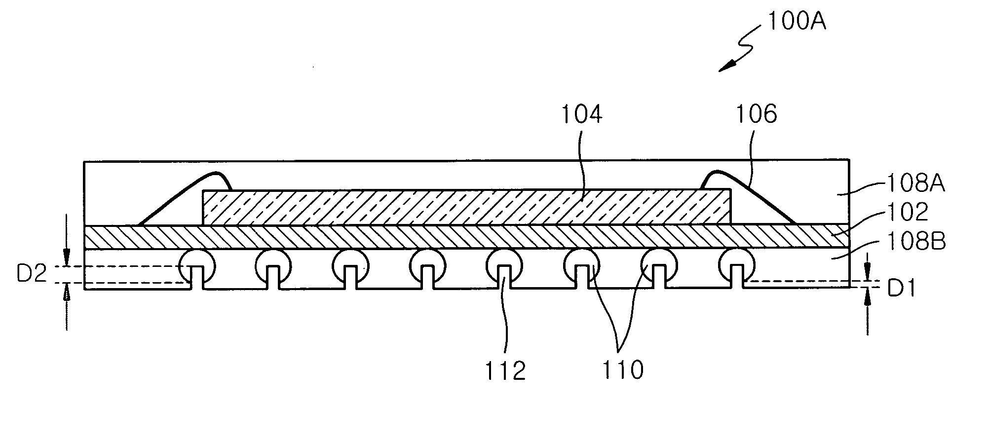
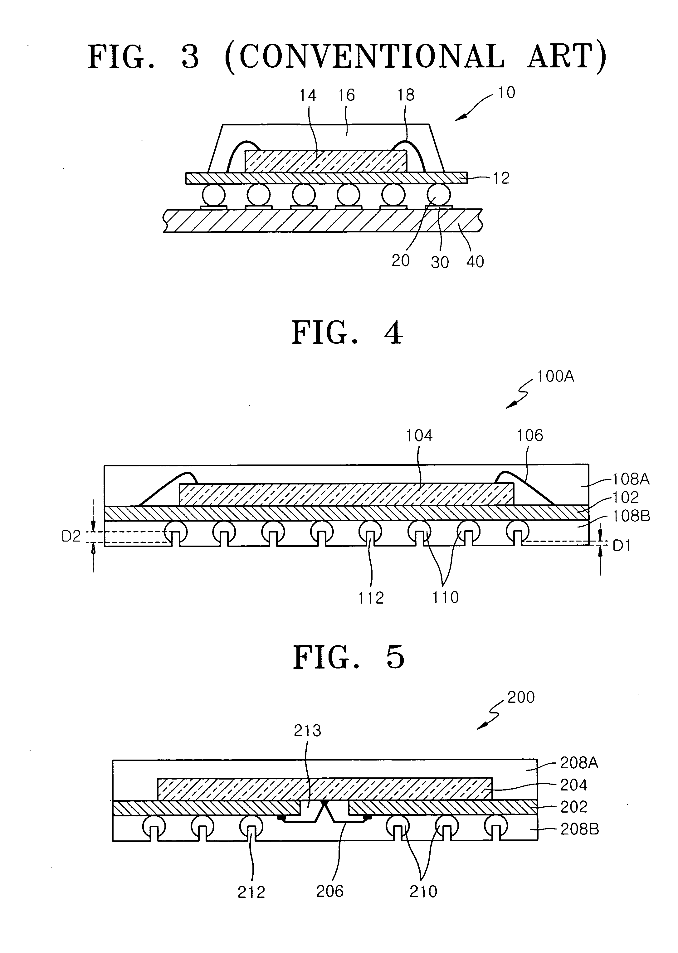
[0028] Example embodiments of the present invention are described more fully hereinafter with reference to the accompanying drawings, in which example embodiments of the present invention are shown. The present invention may, however, be embodied in many different forms and should not be construed as limited to the example embodiments set forth herein. Rather, these example embodiments are provided so that this disclosure will be thorough and complete, and will fully convey the scope of the present invention to those skilled in the art. In the drawings, the sizes and relative sizes of layers and regions may be exaggerated for clarity.

[0029] It will be understood that when an element or layer is referred to as being “on”, “connected to” or “coupled to” another element or layer, it can be directly on, connected or coupled to the other element or layer or intervening elements or layers may be present. In contrast, when an element is referred to as being “directly on,”“directly connect...


PUM


Abstract

A board structure, a ball grid array (BGA) package and method thereof and a solder ball and method thereof. The example solder ball may include a solder portion and a grooved connection portion, formed through a partitioning process, configured to fit a corresponding protruding portion on a board. The example BGA package may include a plurality of the example solder balls. The example board structure may include the example BGA package connected to the board via the grooved connection portions and the protruding portions.

Description

PRIORITY STATEMENT [0001] This application claims benefit of priority under 35 USC § 119 from Korean Patent Application No. 10-2005-0106358, filed on Nov. 8, 2005, in the Korean Intellectual Property Office, the contents of which are incorporated herein by reference in its entirety. BACKGROUND OF THE INVENTION 1. Field of the Invention [0002] Example embodiments of the present invention relate generally to a board structure, a ball grid array (BGA) package and method thereof and a solder ball and method thereof. 2. Description of the Related Art [0003] Conventional leads may be used as external connection terminals for semiconductor packages. More recently, ball-grid array (BGA) packages, which may include solder balls, may be employed instead of leads as external connection terminals. Conventional BGA packages may include a higher fabrication density (e.g., a higher number of external connection terminals in a smaller surface area) as compared to conventional lead packages, and fur...

Claims


Application Information

Patent Timeline
Patent Type & Authority Applications(United States)
IPC IPC(8): H01L23/48
CPCH01L23/49816H01L2224/16H01L2224/4824H01L2924/01079H01L2924/15311H05K3/3436H05K2201/09745H05K2201/10977H05K2203/0465H01L2224/45144H01L2924/00H01L24/48H01L2924/1815H01L2924/00014H01L24/45Y02P70/50H01L2224/05599H01L23/12
Inventor KIM, SHIN
Owner SAMSUNG ELECTRONICS CO LTD
Why Eureka
Try Eureka