High-reliability application printed circuit board assembly QFN assembling and welding pretreatment method

A printed circuit board, pretreatment technology, applied in printed circuits, manufacturing tools, welding equipment, etc., can solve the problems of low reliability of QFN solder joints, prone to false soldering, etc., to shorten the production cycle, uniform tinning, The effect of improving yield and reliability

Active Publication Date: 2019-11-15
嘉兴军胜电子科技有限公司
View PDF9 Cites 7 Cited by
  • Summary
  • Abstract
  • Description
  • Claims
  • Application Information

AI Technical Summary

Problems solved by technology

[0008] Aiming at the deficiencies in the prior art, the object of the present invention is to provide a kind of highly reliable application printed circuit board assembly QFN assembly soldering pretreatment method, this method can improve the uniformity of tin enamel of QFN pad, especially for

Method used


Image

  • High-reliability application printed circuit board assembly QFN assembling and welding pretreatment method
  • High-reliability application printed circuit board assembly QFN assembling and welding pretreatment method
  • High-reliability application printed circuit board assembly QFN assembling and welding pretreatment method

Examples


Example Embodiment

[0032] The present invention is further illustrated by specific examples below. However, these examples are only used to illustrate the present invention and not to limit the scope of the present invention.
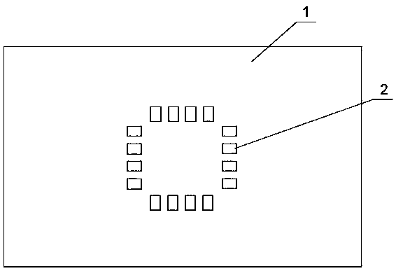
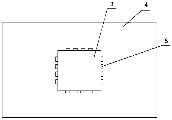
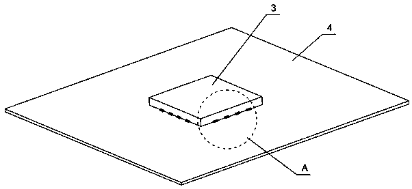
[0033] Attached with instructions Figure 1~5 , A method for pre-enamelling QFN pads, including the following steps:

[0034] Step 1). Fabrication of a carrier board 4 for pre-painting the QFN chip pad 6 with tin. The carrier board 4 is a composite layer structure. The carrier board 4 is a solder mask layer 9 and an FR-4 ring from top to bottom. Oxygen board 7, copper foil layer 8 and FR-4 epoxy board 7; wherein, the solder resist layer 9 is the layer of printed solder paste 5; this design is to meet the needs of this method, and the carrier board is required to be flat and the surface of the carrier board It is not combined with solder, and the carrier board does not deform during heating up to 245°C, while considering processing convenience, low cost and reusability.

[003...


PUM

PropertyMeasurementUnit
Thicknessaaaaaaaaaa

Abstract

The invention discloses a high-reliability application printed circuit board assembly QFN assembling and welding pretreatment method. The method comprises the following steps that 1) a carrying plateis manufactured; 2), a mesh plate is manufactured, at least one through hole corresponding to a QFN chip bonding pad is formed in the mesh plate, and the through holes form a through hole array; 3) dehumidification treatment is carried out on a QFN chip; 4), the mesh plate and the carrying plate are cleaned; 5) the mesh plate is placed on the carrying plate, and a soldering paste containing a soldering flux is printed on the carrying plate through the through hole array; 6) the QFN chip is pasted on the carrying plate with the soldering paste by a chip mounter; 7) hot air reflow soldering processing is performed on the carrying plate pasted with the QFN chip; and 8) the carrying plate pasted with the QFN chip is immersed into a cleaning agent so as to dissolve the soldering flux residue, and the QFN chip is separated from the carrying plate to complete the pre-tin coating. According to the method, the weldability of the QFN chip bonding pad is better through the pre-tin coating treatment, the welding qualification rate and reliability of the QFN chip can be improved, the stability and the service life of the printed circuit board assembly with high reliability are improved, and themaintenance cost of the system is reduced.

Description

technical field [0001] The invention relates to a printed circuit board manufacturing process, in particular to a high-reliability application printed circuit board component QFN assembly welding pretreatment method. Background technique [0002] With the development of multi-function and miniaturization of electronic products, the core of electronic product function realization - the density of printed circuit board components is getting higher and higher, which requires the electronic components used in them to be smaller in size and more comprehensive in functions; QFN (Quad Flat No-lead Package) chips with small size, light weight, low cost and outstanding electrical and thermal properties have become one of the most widely used surface mount devices. [0003] In the prior art, there are many welding methods for QFN chips. For example, the invention application with the application number of 2017105705 19.7 discloses a QFN chip, including a chip body, the chip body is p...

Claims


Application Information

Patent Timeline
IPC IPC(8): B23K1/20B23K1/00
CPCB23K1/0008B23K1/20B23K2101/42
Inventor 陈甲强邱雪晖严慧陈礼峰顾云峰
Owner 嘉兴军胜电子科技有限公司
Why Eureka
Try Eureka