Semiconductor chip package and multichip package

a technology of semiconductor chips and multi-chip packages, which is applied in the direction of semiconductor devices, semiconductor/solid-state device details, electrical apparatus, etc., can solve the problems of deterioration of package reliability, cracks in semiconductor chips, and accompanied multi-chip packages of conventional stack types, so as to improve reliability, shorten the length of bonding wires, and reduce the height

Active Publication Date: 2005-06-30
LAPIS SEMICON CO LTD
View PDF8 Cites 115 Cited by
  • Summary
  • Abstract
  • Description
  • Claims
  • Application Information

AI Technical Summary

Benefits of technology

[0042] As a result, the length of each bonding wire can be shortened and the height thereof can be lowered, as compared with the case in which the bonding wires directly connect between the respective semiconductor chips and the substrate.
[0043] Thus, a wire layout free of contact between the plural bonding wires can be realized. Hence, the occurrence of a malfunction due to a short, a break or the like caused by wire shifting or flowage can be suppressed.
[0044] It is thus possible to realize a multichip package having higher reliability as compared with the conventional one.

Problems solved by technology

However, the conventional stack type multichip package was accompanied by problems to be described below.
There may be a case in which since the bending strength of the semiconductor chip is weak, the force of bonding between electrode pads and bumps becomes insufficient upon bonding, thus resulting in deterioration in package reliability.
There may be a case in which since the bending strength of each semiconductor chip is weak upon sealing the semiconductor chips stacked on the substrate with a resin, cracks occur in the semiconductor chips due to stress concentration caused by a filler contained in a sealing or encapsulating material.
Further, when the semiconductor chips and the leads or substrate are respectively directly connected by bonding wires, the bonding wires become long in length.
Consequently, there may be cases in which the wires are brought into contact with one another, thus causing malfunctions such as a short, breaking, etc.
Since, however, the thickness of the package increases in such a case, the present method is not fit for thinning of the package.

Method used


Image

  • Semiconductor chip package and multichip package
  • Semiconductor chip package and multichip package
  • Semiconductor chip package and multichip package

Examples


first embodiment

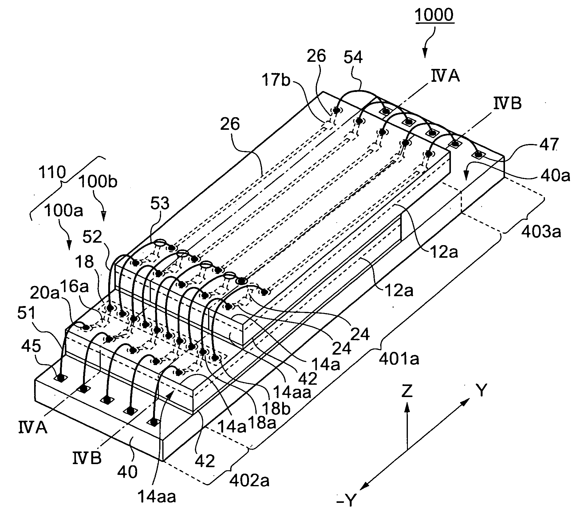
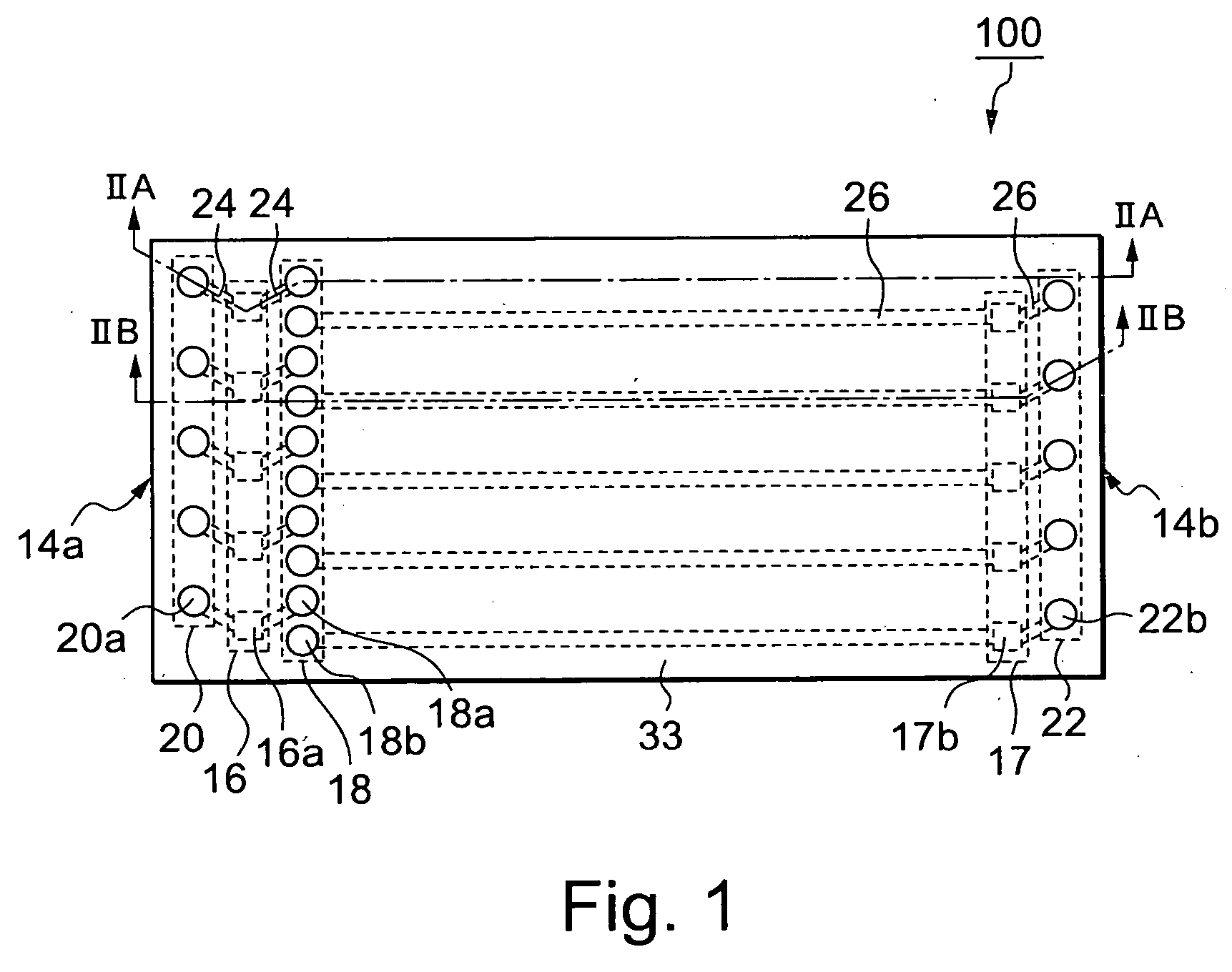
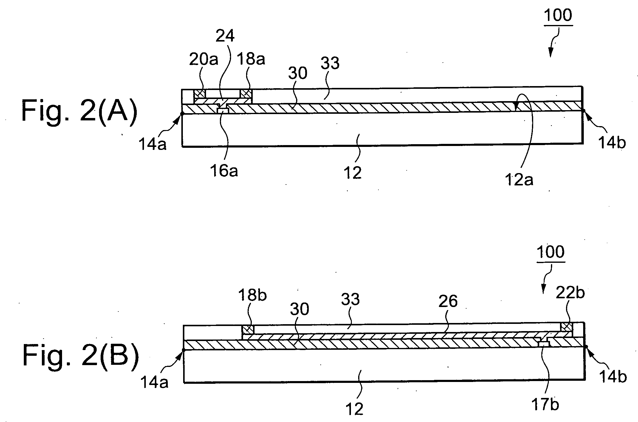
[0059] A semiconductor chip package and a multichip package according to a first embodiment of the present invention will be explained with reference to FIGS. 1 through 4.

[0060]FIG. 1 is a plan view schematically showing one configurational example of a semiconductor chip package 100 according to the present embodiment. FIG. 2(A) is a schematic view showing a cut-away portion (i.e., section) obtained by cutting FIG. 1 along broken line IIA-IIA of FIG. 1. FIG. 2(B) is a schematic view showing a cut-away portion obtained by cutting FIG. 1 along broken line IIB-IIB of FIG. 1. FIG. 3 is a perspective view schematically showing one configurational example of a multichip package 1000 according to the present embodiment. FIG. 4(A) is a schematic view showing a cut-away portion obtained by cutting FIG. 3 along broken line IVA-IVA of FIG. 3. FIG. 4(B) is a schematic view showing a cut-away portion obtained by cutting FIG. 3 along broken line IVB-IVB of FIG. 3.

[0061] As shown in FIGS. 1 and...

second embodiment

[0096] A semiconductor chip package and a multichip package according to a second embodiment of the present invention will be explained with reference to FIGS. 5 through 8.

[0097] FIGS. 5(A) and 5(B) are respectively plan views schematically showing one configurational examples of a semiconductor chip structural body 200 and a semiconductor chip package 250 according to the present embodiment. FIG. 6(A) is a schematic cross-sectional view showing a cut-away portion obtained by cutting FIG. 5(A) along broken line VIA-VIA of FIG. 5(A). FIG. 6(B) is a schematic cross-sectional view showing a cut-away portion obtained by cutting FIG. 5(B) along broken line VIB-VIB of FIG. 5(B). FIG. 7(A) is a perspective view schematically showing one configurational example of a multichip package 2000 according to the present embodiment. FIG. 7(B) is a perspective view of the multichip package 2000 as viewed from its back side. FIG. 8 is a schematic cross-sectional view showing a cut-away portion obtai...

third embodiment

[0127] A semiconductor chip package and a multichip package according to a third embodiment of the present invention will be explained with reference to FIGS. 9(A) and 9(B) through FIG. 12.

[0128] FIGS. 9(A) and 9(B) are respectively plan views schematically showing one configurational examples of a first semiconductor chip package 300 and a second semiconductor chip package 350 according to the present embodiment. FIG. 10(A) is a schematic cross-sectional view showing a cut-away portion obtained by cutting FIG. 9(A) along broken line XA-XA of FIG. 9(A). FIG. 10(B) is a schematic cross-sectional view showing a cut-away portion obtained by cutting FIG. 9(B) along broken line XB-XB of FIG. 9(B). FIG. 11(A) is a perspective view schematically showing one configurational example of a multichip package 3000 according to the present embodiment. FIG. 11(B) is a perspective view of the multichip package 3000 as viewed from its back side. FIG. 12 is a schematic cross-sectional view showing a...


PUM


Abstract

The present invention provides a multichip package wherein a plurality of semiconductor chip packages (100) in each of which first electrode pads (16a) provided in a main surface of a semiconductor chip, and first bonding pads (20a) and first central bonding pads (18a) formed in an upper area of the main surface are respectively electrically connected by first redistribution wiring layers (24) in a one-to-one correspondence relationship, and second electrode pads (17b), and second bonding pads (22b) and second central bonding pads (18b) formed in an upper area of the main surface are respectively electrically connected by second redistribution wiring layers (26) in a one-to-one correspondence relationship, are stacked on one another.

Description

BACKGROUND OF THE INVENTION [0001] 1. Field of the Invention [0002] The present invention relates to a semiconductor chip package and a multichip package equipped with a plurality of the semiconductor chip packages. [0003] This is counterpart of and claims priority to Japanese Patent Application No. 429531 / 2003 filed on Dec. 25, 2003, which is herein incorporated by reference. [0004] 2. Description of the Related Art [0005] There has been known a semiconductor chip stack type package wherein a plurality of semiconductor chips are laminated or stacked on one another in one package in their thickness direction with the aim of carrying out high-density packaging based on multifunctioning of a semiconductor device. [0006] As one example of such a semiconductor chip laminated package, may be mentioned, a stack type multichip package. The stack type multichip package has a configuration wherein a plurality of semiconductor chips are mounted on a substrate in a state of being stacked or la...

Claims


Application Information

Patent Timeline
Patent Type & Authority Applications(United States)
IPC IPC(8): H01L25/18H01L21/60H01L23/02H01L23/31H01L23/495H01L23/525H01L25/065H01L25/10H01L25/11
CPCH01L23/3128H01L23/49575H01L23/525H01L24/06H01L25/0657H01L2224/05553H01L2224/05624H01L2224/48091H01L2224/48137H01L2224/48145H01L2224/48227H01L2224/48235H01L2224/48247H01L2225/06506H01L2225/0651H01L2225/06527H01L2225/06541H01L2225/06555H01L2225/06562H01L2924/01004H01L2924/01006H01L2924/01013H01L2924/01014H01L2924/01022H01L2924/01029H01L2924/01079H01L2924/01082H01L2924/014H01L2924/15311H01L24/48H01L2924/01005H01L2924/01033H01L2924/01047H01L2924/01075H01L2224/32145H01L2224/32225H01L2224/32245H01L2224/73265H01L2924/00014H01L2924/00012H01L2924/00H01L2924/181H01L24/73H01L2924/10161H01L2224/023H01L2224/45099H01L2224/45015H01L2924/207H01L2924/0001
Inventor TAKAHASHI, NORIO
Owner LAPIS SEMICON CO LTD
Why Eureka
Try Eureka