Fabrication methods for electronic system modules

a technology of electronic system modules and fabrication methods, which is applied in the direction of resist details, sustainable manufacturing/processing, and final product manufacturing, etc., can solve the problems of not being able to support direct mounting of bumped devices at a pitch of 100 microns, and not being able to meet the requirements of conventional testing methods, etc., to achieve excellent dimensional stability, the effect of avoiding the use of epoxy under layers and reducing

US20050140026A1Inactive Publication Date: 2005-06-30SK HYNIX INC
43 Cites 28 Cited by

Patent Information

Authority / Receiving Office
US · United States
Patent Type
Applications(United States)
Current Assignee / Owner
Publication Date
2005-06-30
Estimated Expiration
Not applicable · inactive patent

Smart Images

  • Figure 1
    Figure 1
  • Figure 2
    Figure 2
  • Figure 3
    Figure 3
Patent Text Reader

Abstract

This specification describes techniques for manufacturing an electronic system module. The module includes flexible multi-layer interconnection circuits with trace widths of 5 microns or less. A glass panel manufacturing facility, similar to those employed for making liquid crystal display, LCD, panels is used to fabricate the interconnection circuits. A polymer base layer is formed on a glass carrier with an intermediate release layer. Alternate layers of metal and dielectric are formed on the base layer, and patterned to create an array of multi-layer interconnection circuits on the glass panel. A thick layer of polymer is deposited on the interconnection circuit, and openings formed at input / output (I / O) pad locations. Solder paste is deposited in the openings to form wells filled with solder. After dicing the glass carrier to form separated interconnection circuits, IC chips are stud bumped and assembled using flip chip bonding, wherein the stud bumps on the components are inserted into corresponding wells on the interconnection circuits. The IC chips are tested and reworked to form tested circuit assemblies. Methods for connecting to testers and to other modules and electronic systems are described. Module packaging layers are provided for hermetic sealing and for electromagnetic shielding. A blade server embodiment is also described.
Need to check novelty before this filing date? Find Prior Art

Description

RELATED APPLICATIONS

[0001] This application claims priority to Provisional Application Ser. No. 60 / 318,271 filed Sep. 7, 2001.BACKGROUND OF THE INVENTION

[0002] 1. Field of the Invention

[0003] This invention relates generally to an electronic system module and method of fabrication, and more particularly to an electronic system module fabricated on a carrier from which it can be released.

[0004] 2. Description of the Related Art

[0005] The number of input / output (I / O) connections required by integrated circuit (IC) chips is increasing, to several hundred for recent microprocessor chips. As verification of complex designs becomes an increasing portion of the total design activity, it is desirable to increase the I / O count further, to provide access to more internal nodes for testing. Flip chip assembly methods have helped to provide more I / O connections because they provide an area array of connections across the entire face of an IC chip, rather than just at the perimeter as with ...

Examples

Embodiment Construction

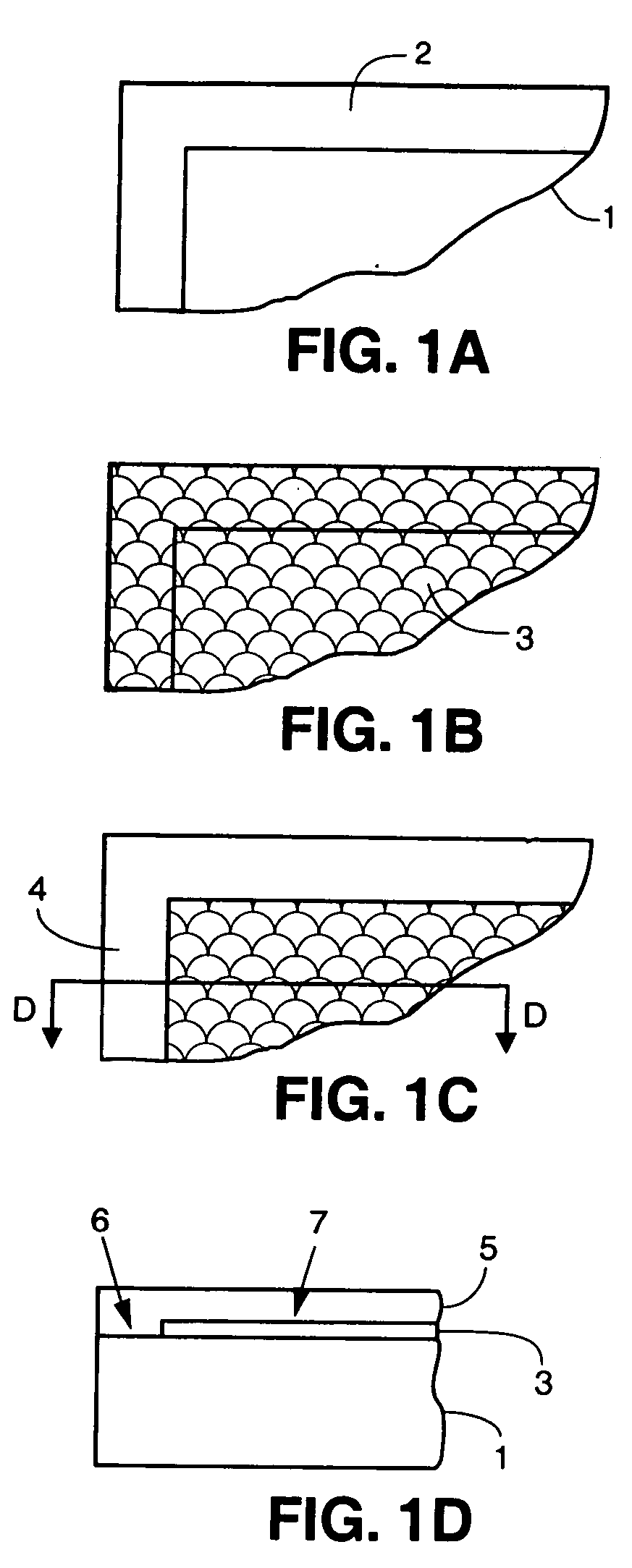
[0054]FIG. 1A shows a corner fragment of a glass carrier 1. Photo resist has been patterned on the carrier, so that a border of resist, 2, having a width of approximately 20 mm, surrounds the perimeter. FIG. 1B shows that a film of release layer, 3, has been applied over the entire surface of the glass carrier. A suitable material for the release layer is a fluorinated silicone such as F065 manufactured by Gelest, Inc., in Morrisville Pa., USA. This material is a single part gel. It can be applied as a fog or fine spray, or using the spin-on method. A suitable thickness is 2-5 microns after curing, with 2 microns preferred. A typical curing cycle is 125° C. for 25 minutes. This release material has a silane component that bonds well to glass surfaces, yet presents a fluid-like interface to polymeric materials like the base layer to be subsequently applied. FIG. 1C shows the result of lifting the resist to pattern the release layer, using a developer or resist stripper to swell the r...