Electron emission device including dummy electrodes
a technology of dummy electrodes and emission devices, which is applied in the manufacture of electric discharge tubes/lamps, tubes with screens, discharge tubes luminescnet screens, etc., can solve the problems of difficult to arrange a getter with a predetermined volume, easy to occur signal distortion, etc., to prevent the quality of the screen from deteriorating, the effect of inhibiting signal distortion
- Summary
- Abstract
- Description
- Claims
- Application Information
AI Technical Summary
Benefits of technology
Problems solved by technology
Method used
Image

Examples
first embodiment
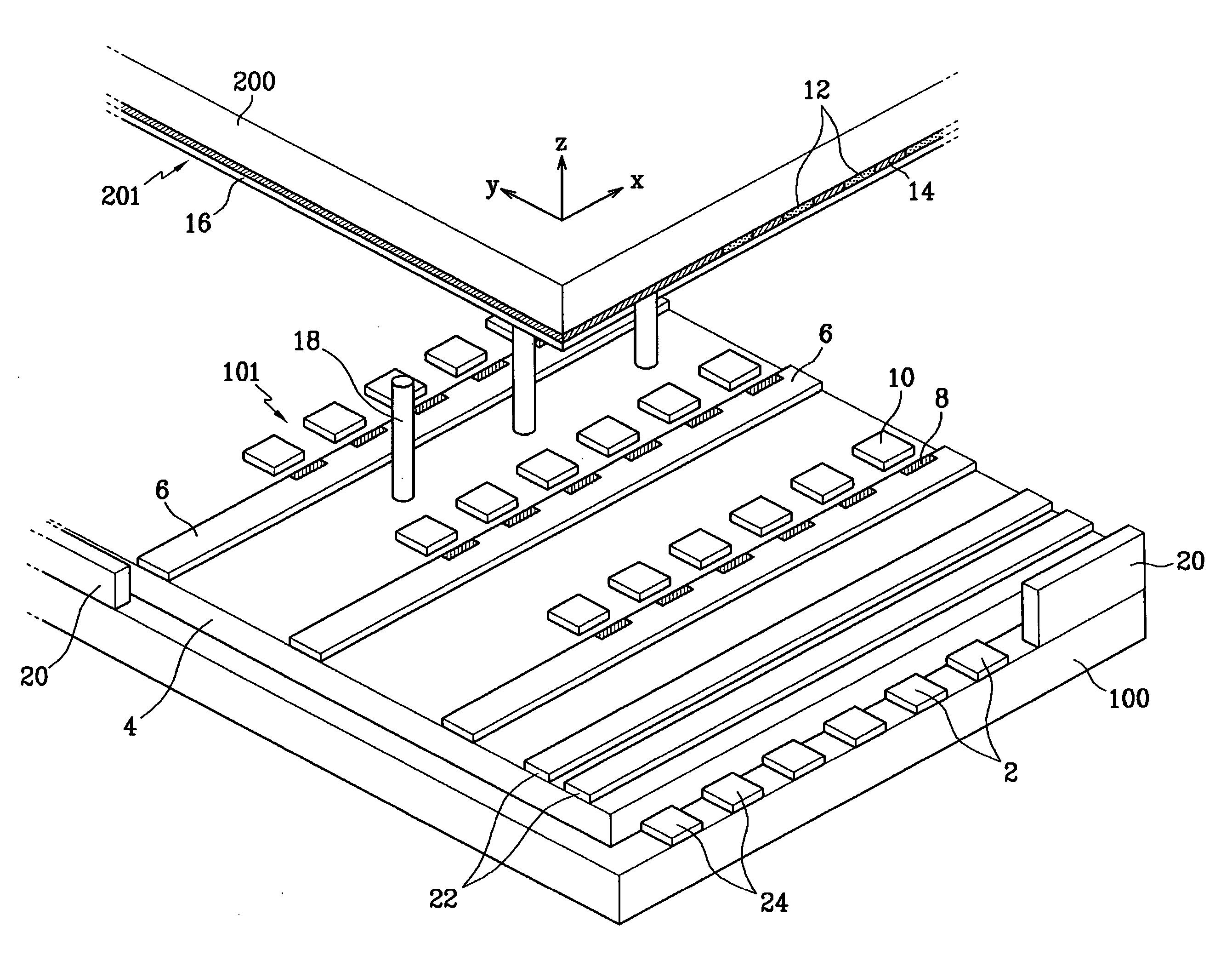
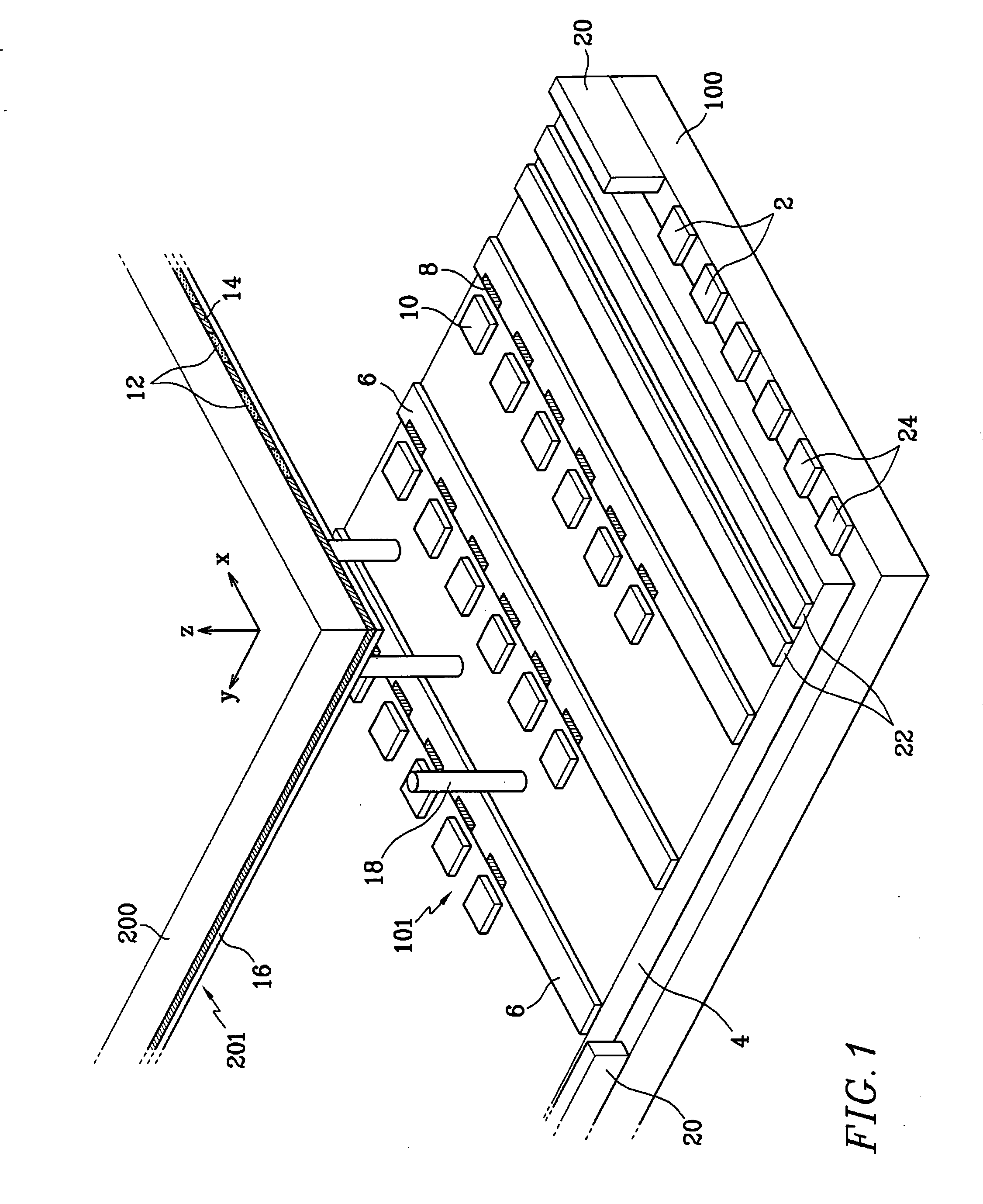
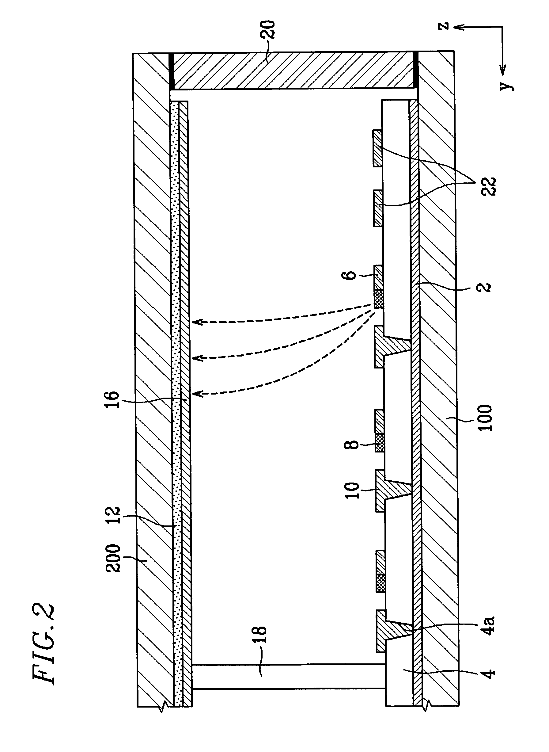
[0042]FIG. 1 is a partial exploded perspective view of an electron emission device according to the present invention, and FIG. 2 is a partial sectional view of the electron emission device, illustrating the combinatorial state thereof.
[0043] As shown in the drawings, the electron emission device includes first and second substrates 100 and 200 facing each other with a distance while forming a vacuum vessel. An II electron emission unit 101 is provided on the first substrate 100 to emit electrons under the application of an electric field, and a light emission unit 201 is formed on the second substrate 200 to radiate visible rays due to the electrons emitted from the electron emission unit 101.
[0044] Specifically, gate electrodes 2 are line-patterned on the first-substrate 100 in one direction (in the Y direction of the drawing), and an insulating layer 4 is formed on the entire surface of the first substrate 100 while covering the gate electrodes 2. Cathode electrodes 6 are line-p...
second embodiment
[0062]FIG. 5 is a partial exploded perspective view of an electron emission device according to the present invention, and FIG. 6 is a partial sectional view of the electron emission device, illustrating the combinatorial state thereof.
[0063] As shown in the drawings, opening portions 40 are formed at the gate electrodes 30 and the insulating layer 32 per the respective pixel regions where the cathode electrodes 34 and the gate electrodes 30 cross each other. The opening portions 40 partially expose the cathode electrodes 34, and electron emission regions 42 are formed on the cathode electrodes 34 within the opening portions 40. A first dummy electrode 36 is placed external to the outermost gate electrode 30 parallel thereto, and a second dummy electrode 38 is placed external to the outermost cathode electrode 34 parallel thereto.
[0064] With the above structure, scan signals are applied to the gate electrodes 30, and data signals are applied to the cathode electrodes 34. The pixel ...
fourth embodiment
[0072]FIG. 10 is a partial plan view of a first substrate of an electron emission device according to the present invention.
[0073] As shown in FIG. 10, getter layers 48 are formed at one side periphery of a first dummy electrode 50 facing counter electrodes 10. Preferably, the first dummy electrode 50 has a width larger than that of the cathode electrode 6 to increase the number of the getter layers 48. The portions of the first dummy electrode 50 crossing over the gate electrodes 2 are removed to form opening portions 50a exposing the insulating layer 4, and a getter layer 48 is formed at one side periphery of each opening portion 50a.
[0074] Consequently, the amount of the electron emission material of the getter layers 48 formed on the first dummy electrode 50 is larger than that of the electron emission regions 8 formed on the cathode electrodes 6, thereby heightening the remnant gas collection efficiency.
[0075] With the electron emission device according to the present embodim...
PUM
 Abstract
Description
Claims
Application Information
 - R&D
- Intellectual Property
- Life Sciences
- Materials
- Tech Scout
- Unparalleled Data Quality
- Higher Quality Content
- 60% Fewer Hallucinations
Browse by: Latest US Patents, China's latest patents, Technical Efficacy Thesaurus, Application Domain, Technology Topic, Popular Technical Reports.
© 2025 PatSnap. All rights reserved.Legal|Privacy policy|Modern Slavery Act Transparency Statement|Sitemap|About US| Contact US: help@patsnap.com