

Circuit array substrate and flat panel display device provided with the same
- Summary
- Abstract
- Description
- Claims
- Application Information
AI Technical Summary
Benefits of technology
Problems solved by technology
Method used
Image

Examples
first embodiment
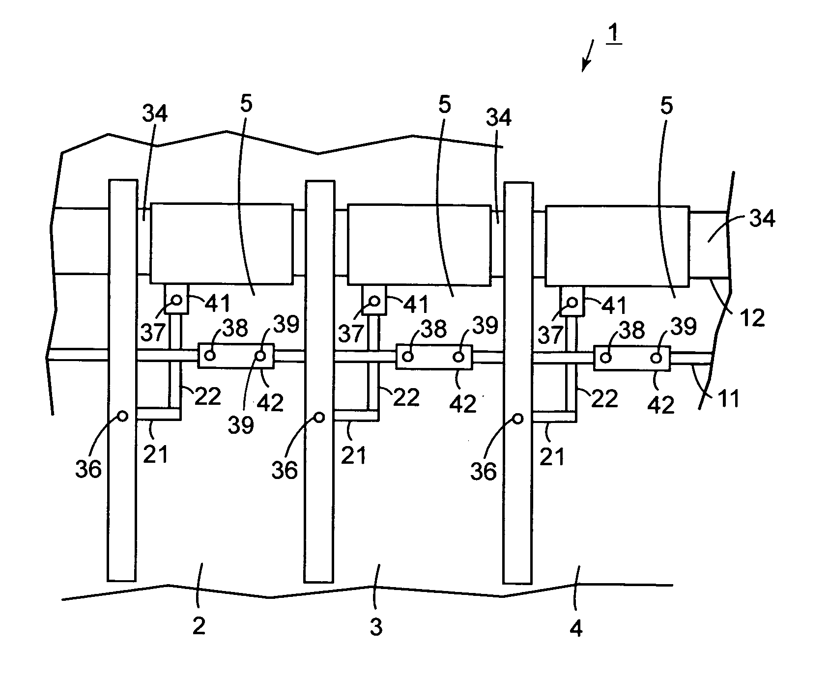
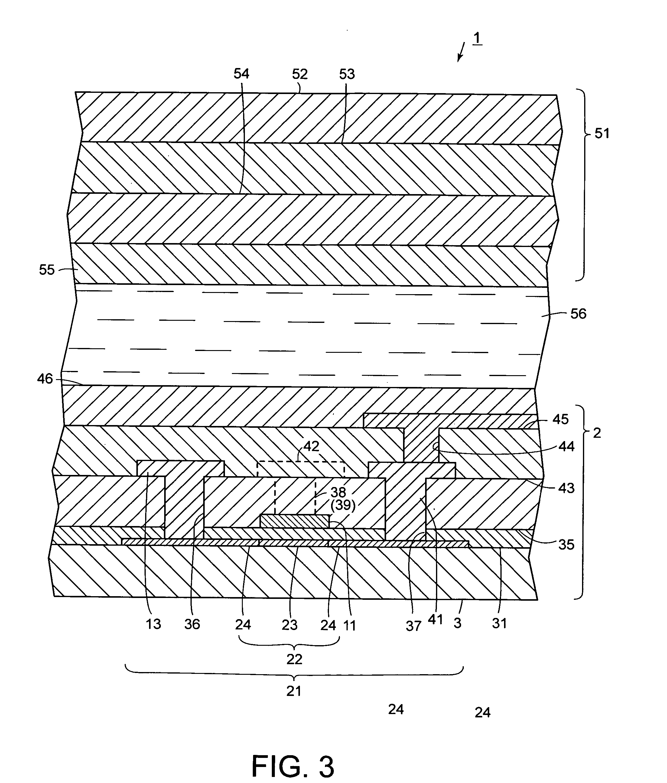
[0022] A flat panel display device such as a liquid crystal display device of the first embodiment in accordance with the present invention will be described below with reference to FIGS. 1-3.
[0023] Liquid crystal display device 1 shown in FIGS. 1-3 includes top gate type or reverse-stagger type polycrystalline silicon thin-film transistors. Further, liquid crystal display device 1 is an AMLCD provided with a substantially rectangular plate-like circuit array substrate 2. Circuit array substrate 2 has glass substrate 3 which is substantially rectangular and optically transparent but electrically insulated. One main surface of glass substrate 3 includes substantially rectangular display region 4 formed on its major portion. Display region 4 is provided with a plurality of pixels 5 disposed in a dotted matrix.
[0024] Further, display region 4 of glass substrate 3 contains gate electrode lines 11, i.e., gate electrodes of thin-film transistors and scanning lines connected to the gate e...
second embodiment
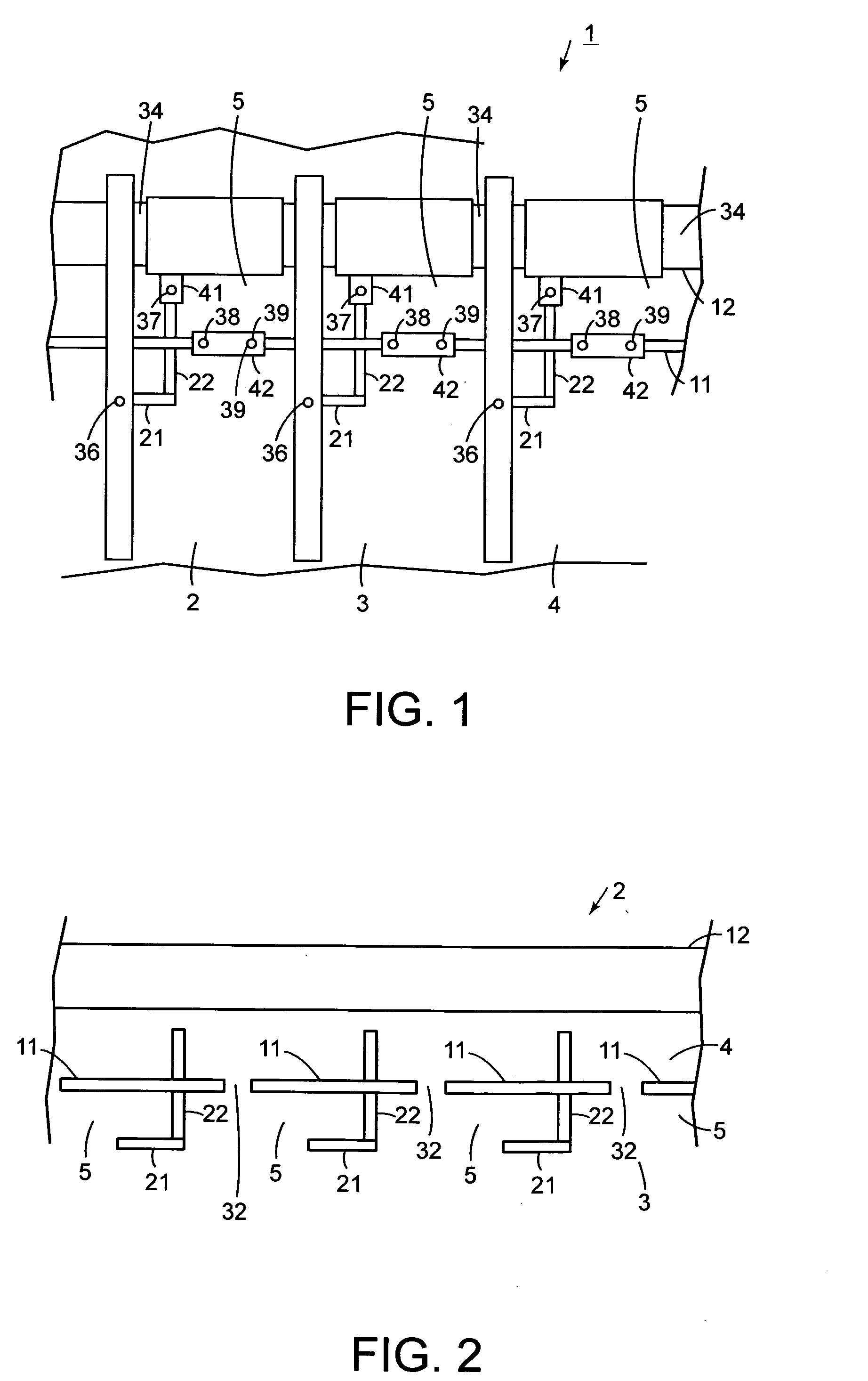
[0067] Next, the present invention will be described below with reference to FIGS. 4 and 5.
[0068] Liquid crystal display device 1 shown in FIGS. 4 and 5 is basically the same as liquid crystal display device 1 shown in FIGS. 1-3 but separating portions 32 are provided not for every pixel 5 but for a plurality of pixels 5. Separating portions 32 are disposed at respective pixels 5 of a predetermined color, for instance.
[0069] Here, dummy patterns 71 are prepared for pixels 5 where no separating portions 32 are formed. Dummy patterns 71 are the same in structure as conductive films 42. Both conductive films 42 and dummy patterns are formed on interlayer insulation film 35 which is different from gate insulation film 31 on which gate electrode lines 11 are formed. Both end portions of each conductive film 42 and dummy pattern 71 are electrically connected to gate electrode line 11 through contact holes 72.
[0070] Thus, even though separating portion 32 are provided only for every pred...
PUM
 Abstract
Description
Claims
Application Information