Device isolation method of semiconductor memory device and flash memory device fabricating method using the same

Inactive Publication Date: 2005-06-30
DONGBU HITEK CO LTD
View PDF2 Cites 4 Cited by
  • Summary
  • Abstract
  • Description
  • Claims
  • Application Information

AI Technical Summary

Benefits of technology

[0012] Another object of the present invention is to provide a flash memory device fabricating method, which can prevent a bridge occurrence between cells due to a residue o

Problems solved by technology

Yet, in the related art floating gate forming method, it is difficult to precisely pattern the floating gate due to the misalignment between the device isolation layer and the etch mask for patterning the floating gate, i.e., the photoresist pattern.
Hence, limitation is put on

Method used


Image

  • Device isolation method of semiconductor memory device and flash memory device fabricating method using the same
  • Device isolation method of semiconductor memory device and flash memory device fabricating method using the same
  • Device isolation method of semiconductor memory device and flash memory device fabricating method using the same

Examples


Example

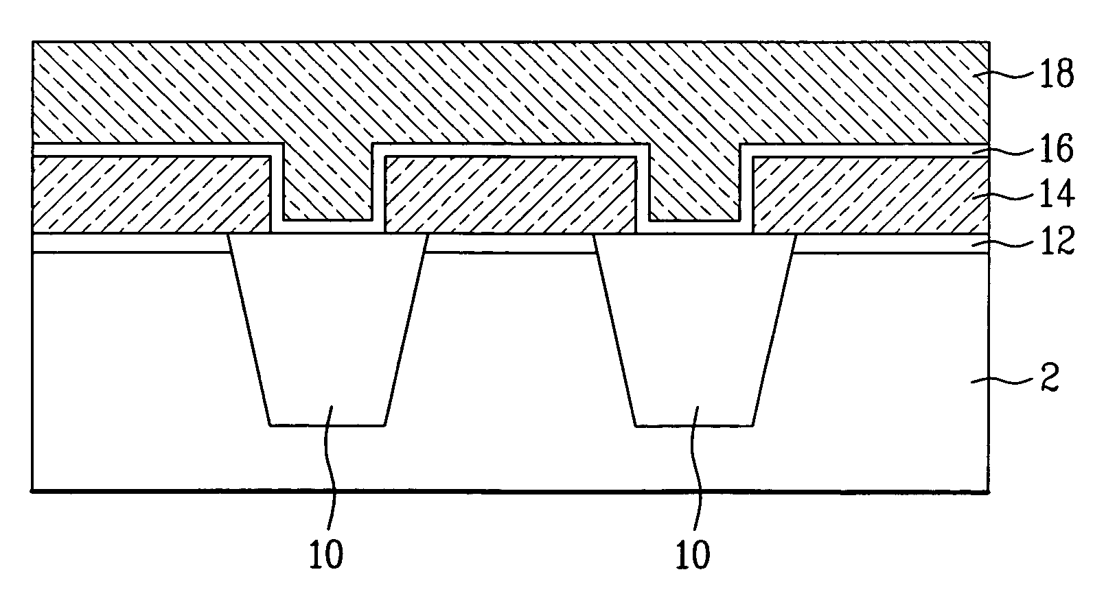
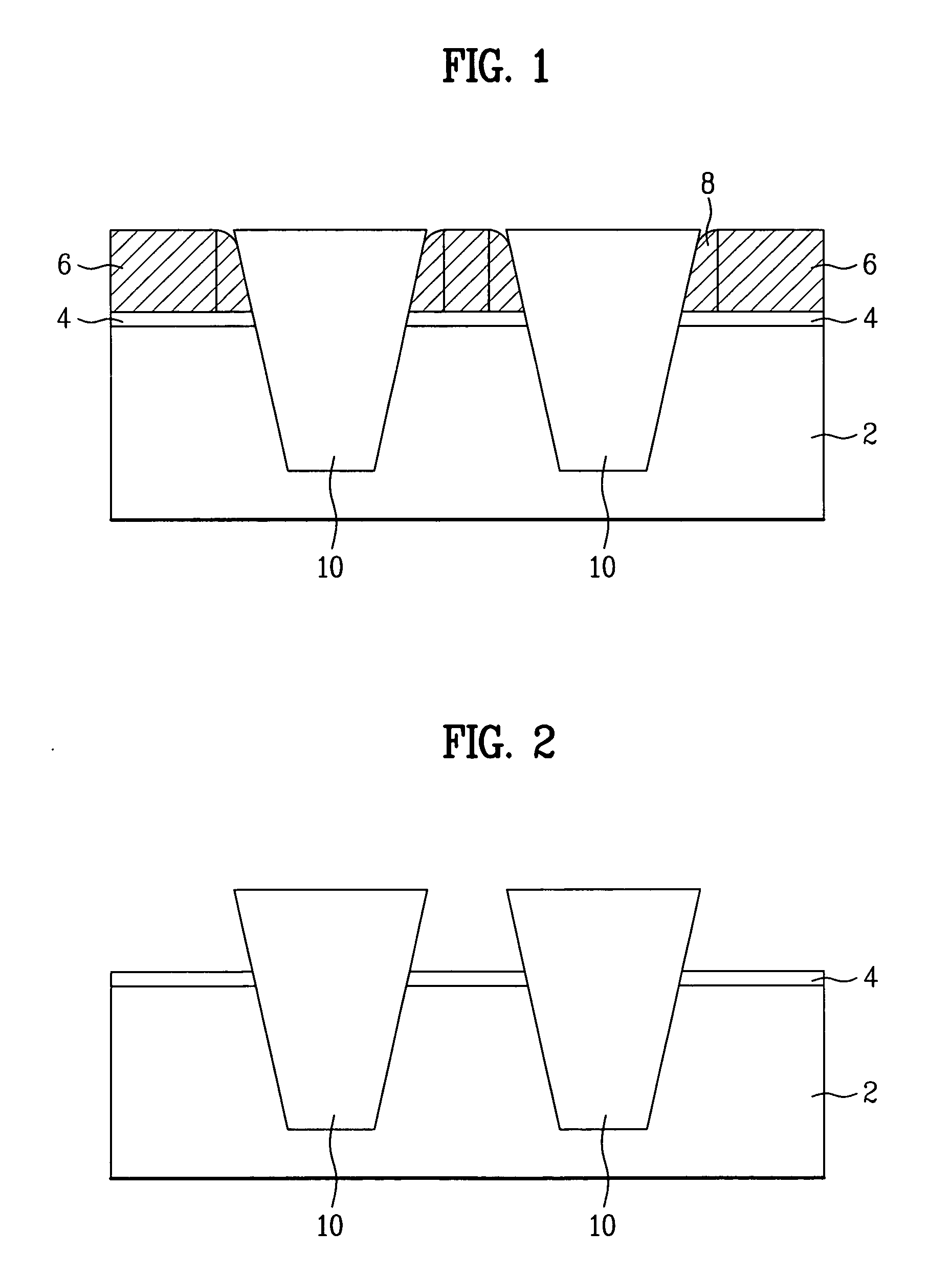
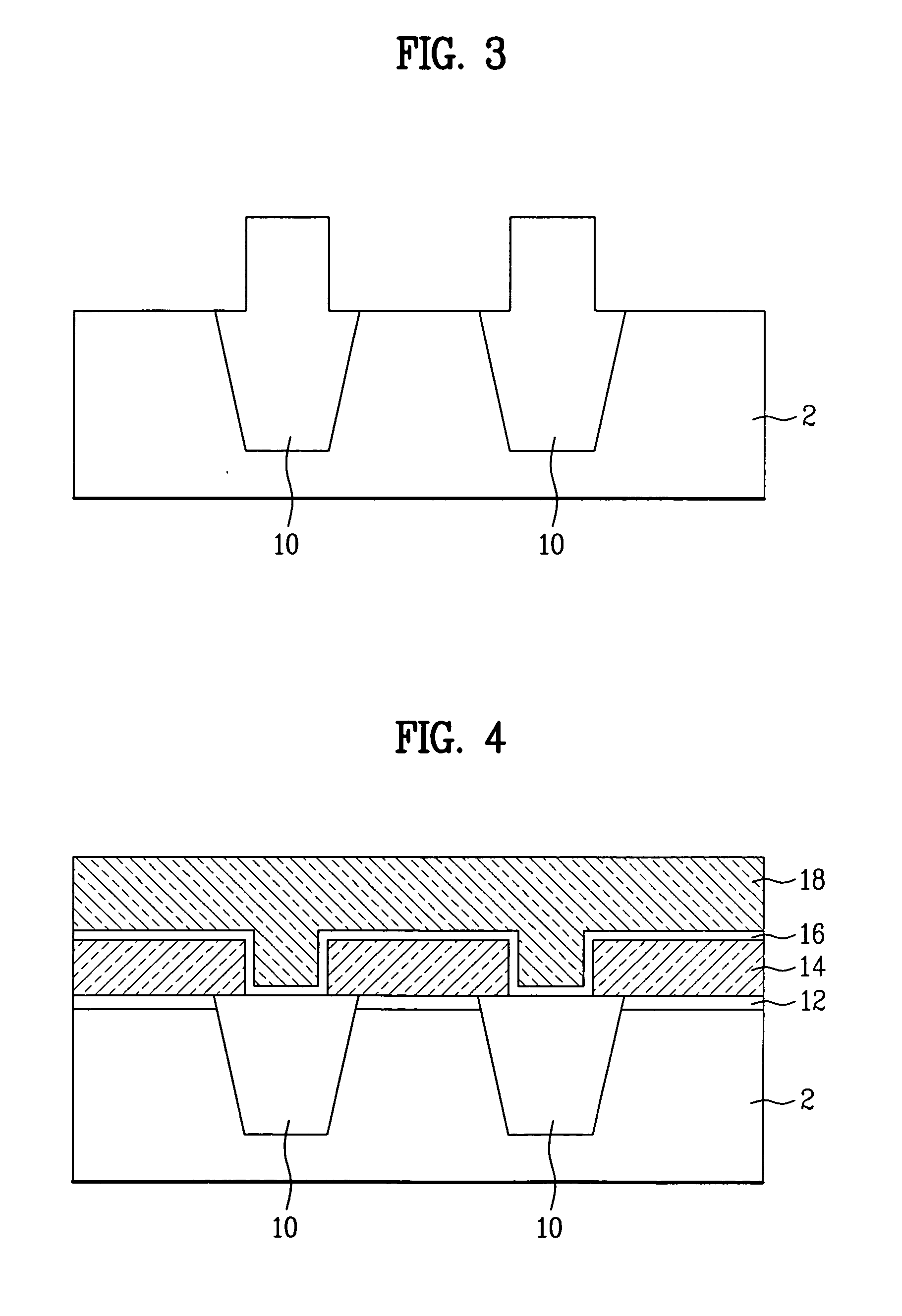
[0025] Reference will now be made in detail to the preferred embodiments of the present invention, examples of which are illustrated in the accompanying drawings. Wherever possible, the same reference numbers will be used throughout the drawings to refer to the same or like parts.

[0026] FIGS. 1 to 4 are cross-sectional diagrams for explaining a device isolation method of a semiconductor memory device and flash memory device fabricating method using the same according to the present invention.

[0027] Referring to FIG. 1, a pad oxide layer 4 is formed on a semiconductor substrate 2 by growing an oxide layer thereon. And, a nitride layer 6 is deposited on the pad oxide layer 4. In doing so, the nitride layer 46 is formed 1,500˜4,500 Å thick.

[0028] A photoresist pattern (not shown in the drawing) exposing an area for forming a trench therein is formed on the nitride layer 6.

[0029] The nitride layer and the oxide layer are sequentially etched to expose the semiconductor substrate 2 wh...


PUM


Abstract

The present invention provides a device isolation method of a semiconductor memory device and flash memory device fabricating method using the same, which can prevent a bridge occurrence between cells. The present invention includes forming a nitride layer pattern defining a trench forming area on a semiconductor substrate, forming a spacer on a sidewall of the nitride layer pattern, forming a trench in the semiconductor layer by removing a portion of the semiconductor layer using the nitride layer pattern and the spacer as an etch mask, forming a device isolation layer filling up the trench, removing the nitride layer pattern and the spacer to complete the device isolation layer, forming a conductor layer over the substrate including the device isolation layer, planarizing the conductor layer and the device isolation layer to lie in a same plane, and forming an insulating layer over the substrate.

Description

[0001] This application claims the benefit of the Korean Application No. P2003-0098359 filed on Dec. 27, 2003, which is hereby incorporated by reference. BACKGROUND OF THE INVENTION [0002] 1. Field of the Invention [0003] The present invention relates to a device isolation method of a semiconductor memory device and flash memory device fabricating method using the same, by which characteristics of the semiconductor memory device can be enhanced. [0004] 2. Discussion of the Related Art [0005] Generally, in forming floating gates for fabricating a slash memory device, it is important to electrically separate the floating gates in neighbor cells. [0006] A floating gate is formed in a manner of forming a device isolation layer by shallow trench isolation (hereinafter abbreviated STI), forming a tunnel oxide layer by depositing an oxide layer over a substrate, depositing a doped polysilicon layer on the tunnel oxide layer, and patterning the doped polysilicon layer. [0007] Yet, in the re...

Claims


Application Information

Patent Timeline
IPC IPC(8): H01L21/762H01L21/8247H01L27/115
CPCH01L21/76224H01L27/11521H01L27/115H10B69/00H10B41/30H01L21/762
Inventor JUNG, SUNG MUNKIM, JUM SOO
Owner DONGBU HITEK CO LTD
Why Eureka
Try Eureka