Semiconductor memory device having advanced tag block

Inactive Publication Date: 2005-06-30
SK HYNIX INC
View PDF21 Cites 7 Cited by
  • Summary
  • Abstract
  • Description
  • Claims
  • Application Information

AI Technical Summary

Benefits of technology

[0045] It is, therefore, an object of the present invention to provide a semiconductor memory device, for accessing data on high speed, having a tag block which is constituted with single row decoder so that a circuit size of the semiconductor memory device is reduced and a control of a data access operation is more simplified.

Problems solved by technology

As a result, many problems may arise because the operation speed of the memory device is slower than that of CPU.
However, the predetermined word lines are not fixed but changed during an operation of the memory device.
As above described, though the semiconductor memory device having the tag block can perform a data access operation on high speed because the data stored in each unit cell block is continuously accessed, the tag block having a row address decoding block for controlling the data access operation is much complicated; and a size of the tag block is dramatically increased.

Method used


Image

  • Semiconductor memory device having advanced tag block
  • Semiconductor memory device having advanced tag block
  • Semiconductor memory device having advanced tag block

Examples


Embodiment Construction

[0059] Hereinafter, a semiconductor memory device having an advanced tag block according to the present invention will be described in detail referring to the accompanying drawings.

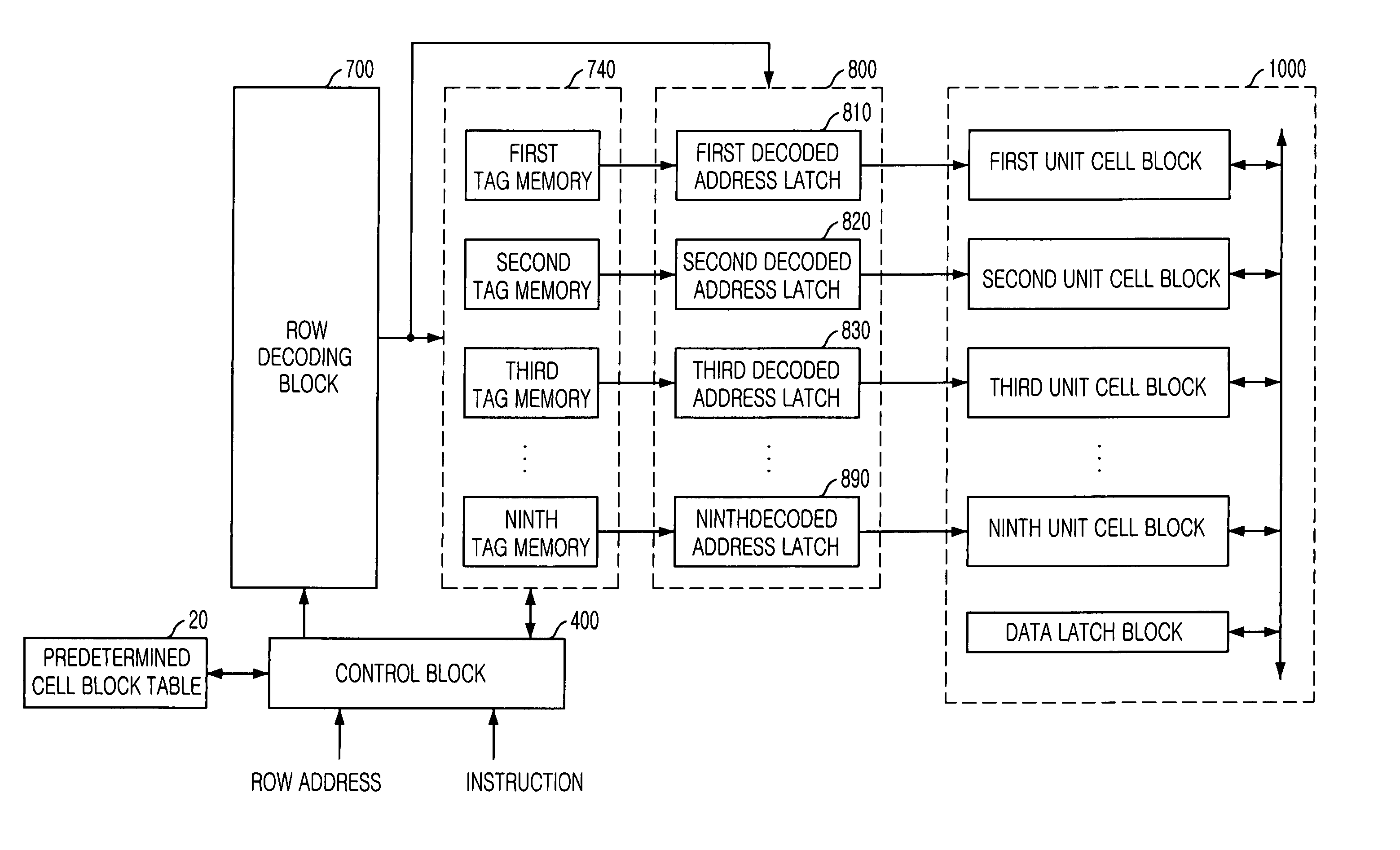
[0060]FIG. 8 is a block diagram showing a semiconductor memory device in accordance with the present invention.

[0061] As shown, the semiconductor memory device includes a control block 400, a predetermined cell block table 20, a row decoding block 700, a tag memory block 740, a decoded address latching block 800 and a cell area 1000.

[0062] The cell area 1000 has N+1 number of unit cell blocks, e.g., first to ninth unit cell blocks, each including 256 number of word lines for responding to an inputted row address. A row address is inputted in response to eight unit cell blocks. Herein, the cell area 1000 further includes additional unit cell block. The predetermined cell block table 20 is used for storing information wherein at least more than one word line among the (8+1)×256 number of the word lines i...


PUM


Abstract

A semiconductor memory device includes a row decoding block for decoding an inputted address to thereby generate a logical unit cell block address and a decoded word line address; a tag block for converting the logical unit cell block address into a physical unit cell block address; a decoded address latching block for latching the decoded word line address to thereby output the decoded word line address as a word line activation signal in response to the physical unit cell block; and a cell area for outputting a data, which is stored therein, in response to the word line activation signal.

Description

FIELD OF INVENTION [0001] The present invention relates to a semiconductor memory device; and, more particularly, to a tag block, for use in the semiconductor memory device, for reducing a data access time. DESCRIPTION OF PRIOR ART [0002] Generally, a semiconductor memory device is classified as a random access memory (RAM) and a read only memory (ROM). [0003] The RAM includes a Dynamic RAM (DRAM) and a Static RAM (SRAM). One cell of the dynamic RAM has one transistor and one capacitor and that of the static RAM does four transistors and two load resistances. The DRAM is used more widespread than the SRAM because the DRAM is more efficient than SRAM in a chip integration and a manufacturing process. [0004] Today, an operation speed of a central processing unit (CPU) is more dramatically advanced than that of the DRAM. As a result, many problems may arise because the operation speed of the memory device is slower than that of CPU. For overcoming these problems, several kinds of schem...

Claims


Application Information

Patent Timeline
IPC IPC(8): G06F12/00G11C7/10G11C15/04G11C8/06
CPCG11C8/06G11C7/10
Inventor HONG, SANG-HOONAHN, JIN-HONGKO, JAE-BUMKIM, SE-JUN
Owner SK HYNIX INC
Why Eureka
Try Eureka