Co-doping for fermi level control in semi-insulating Group III nitrides

a semi-insulating group and nitride technology, applied in the field of semi-insulating group iii nitride semiconductor layers, can solve the problems of different insulating characteristics of the resulting layer, may not be well suited to higher power and/or high frequency applications,

Active Publication Date: 2005-07-07
CREE INC
View PDF14 Cites 37 Cited by
  • Summary
  • Abstract
  • Description
  • Claims
  • Application Information

AI Technical Summary

Benefits of technology

[0007] In additional embodiments of the present invention, a concentration of the shallow level p-type dopant is sufficient to cause a donor-like energy level of the deep level transition metal dopant to be a dominant energy level of the deep level transition metal dopant.

Problems solved by technology

These, more familiar, semiconductor materials may not be well suited for higher power and / or high frequency applications, however, because of their relatively small bandgaps (e.g., 1.12 eV for Si and 1.42 for GaAs at room temperature) and / or relatively small breakdown voltages.
Insulating GaN layers have also been fabricated by doping the GaN layers with Fe or C. While such techniques may produce a semi-insulating Group III nitride layer, variations between production runs may result in differing insulating characteristics of the resulting layers.

Method used


Image

  • Co-doping for fermi level control in semi-insulating Group III nitrides
  • Co-doping for fermi level control in semi-insulating Group III nitrides
  • Co-doping for fermi level control in semi-insulating Group III nitrides

Examples


Embodiment Construction

[0017] The present invention now will be described more fully hereinafter with reference to the accompanying drawings, in which embodiments of the invention are shown. This invention may, however, be embodied in many different forms and should not be construed as limited to the embodiments set forth herein; rather, these embodiments are provided so that this disclosure will be thorough and complete, and will fully convey the scope of the invention to those skilled in the art. Like numbers refer to like elements throughout. As will also be appreciated by those of skill in the art, references herein to a layer formed “on” a substrate or other layer may refer to the layer formed directly on the substrate or other layer or on an intervening layer or layers formed on the substrate or other layer. As used herein the term “and / or” includes any and all combinations of one or more of the associated listed items.

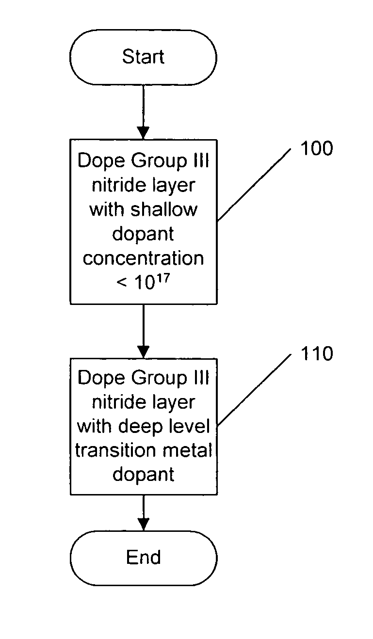
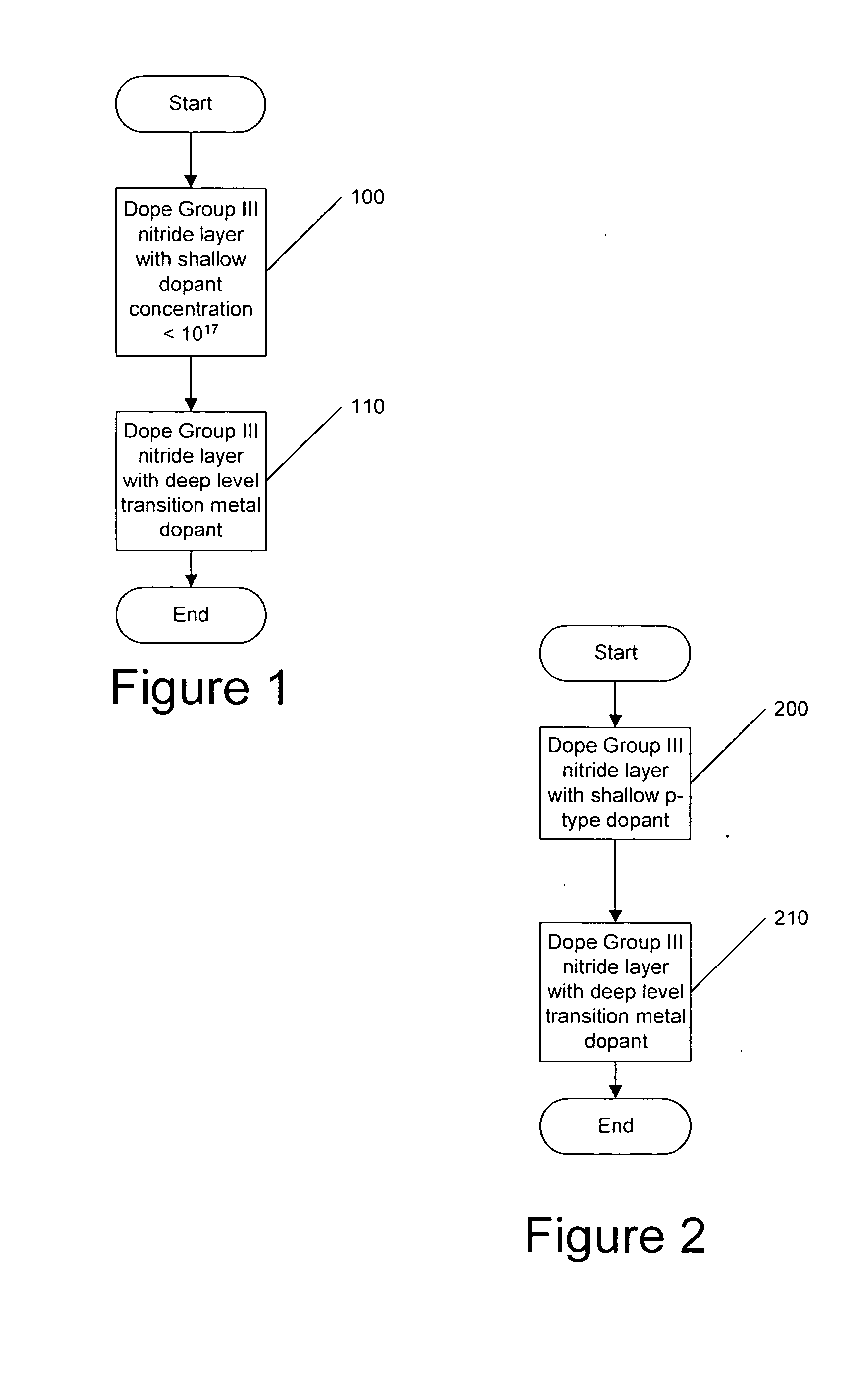
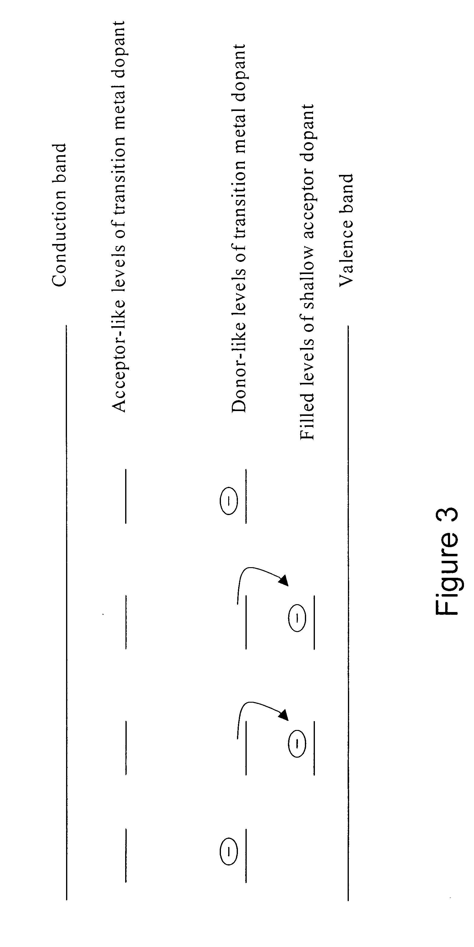
[0018] Embodiments of the present invention may utilize co-doping of a Group III...


PUM

PropertyMeasurementUnit
energy levelaaaaaaaaaa
semi-insulatingaaaaaaaaaa
semiconductoraaaaaaaaaa

Abstract

Semi-insulating Group III nitride layers and methods of fabricating semi-insulating Group III nitride layers include doping a Group III nitride layer with a shallow level p-type dopant and doping the Group III nitride layer with a deep level dopant, such as a deep level transition metal dopant. Such layers and/or method may also include doping a Group III nitride layer with a shallow level dopant having a concentration of less than about 1×1017 cm−3 and doping the Group III nitride layer with a deep level transition metal dopant. The concentration of the deep level transition metal dopant is greater than a concentration of the shallow level p-type dopant.

Description

FIELD OF THE INVENTION [0001] The present invention relates to semiconductor materials and, more particularly, to semi-insulating Group III nitride semiconductor layers. BACKGROUND [0002] Materials such as silicon (Si) and gallium arsenide (GaAs) have found wide application in semiconductor devices for lower power and (in the case of Si) lower frequency applications. These, more familiar, semiconductor materials may not be well suited for higher power and / or high frequency applications, however, because of their relatively small bandgaps (e.g., 1.12 eV for Si and 1.42 for GaAs at room temperature) and / or relatively small breakdown voltages. [0003] In light of the difficulties presented by Si and GaAs, interest in high power, high temperature and / or high frequency applications and devices has turned to wide bandgap semiconductor materials such as silicon carbide (2.996 eV for alpha SiC at room temperature) and the Group III nitrides (e.g., 3.36 eV for GaN at room temperature). These ...

Claims


Application Information

Patent Timeline
Patent Type & Authority Applications(United States)
IPC IPC(8): H01L21/20H01L21/205
CPCH01L21/02378H01L21/02581H01L21/02579H01L21/0254H01L21/20
Inventor SAXLER, ADAM WILLIAM
Owner CREE INC
Why Eureka
Try Eureka