Heterojunction BiCMOS integrated circuits and method therefor

a technology of heterojunction bipolar transistor and integrated circuit, which is applied in the direction of transistors, electrical equipment, solid-state devices, etc., can solve the problems of inherently damaging the semi-conductive layer of the compound, etching polysilicon, and the manufacturing of hbts, and achieves the effect of being suitable for the manufacturing process of bicmos

Inactive Publication Date: 2005-07-07
CHARTERED SEMICONDUCTOR MANUFACTURING
View PDF3 Cites 9 Cited by
  • Summary
  • Abstract
  • Description
  • Claims
  • Application Information

AI Technical Summary

Problems solved by technology

Although the use of compound semiconductive materials has proven useful in HBTs, problems exist in the manufacturing of HBTs.
Several of these processing steps inherently damage the compound semiconductive layer.
Etching polysilicon, for example, adversely affects the compound semiconductive layer beneath the polysilicon because the etchants used do not selectively etch only the polysilicon.
Some of the compound semiconductive layer is also etched during this processing step resulting in HBTs that are relatively slower and exhibit relatively poor electrical noise performance.
However, this technique has the problem of ion channeling, which limits the minimum thickness of the base layer.
Another disadvantage of ion implantation is that the Si / SiGe or Si / SiGeC layer is often damaged by the ions during implantation.
This annealing step, however, alters the concentration profile within the various layers of semiconductive materials that make up the transistor.
Furthermore, the differences in manufacturing techniques used to form CMOS transistors and HBTs have made it difficult to manufacture BiCMOS integrated circuit devices using compound semiconductive materials that have proven to be beneficial in HBTs.
Solutions to these problems have been long sought but prior developments have not taught or suggested any solutions and, thus, solutions to these problems have long eluded those skilled in the art.

Method used


Image

  • Heterojunction BiCMOS integrated circuits and method therefor
  • Heterojunction BiCMOS integrated circuits and method therefor
  • Heterojunction BiCMOS integrated circuits and method therefor

Examples


Embodiment Construction

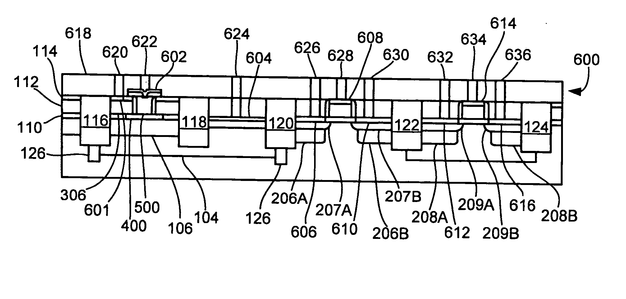
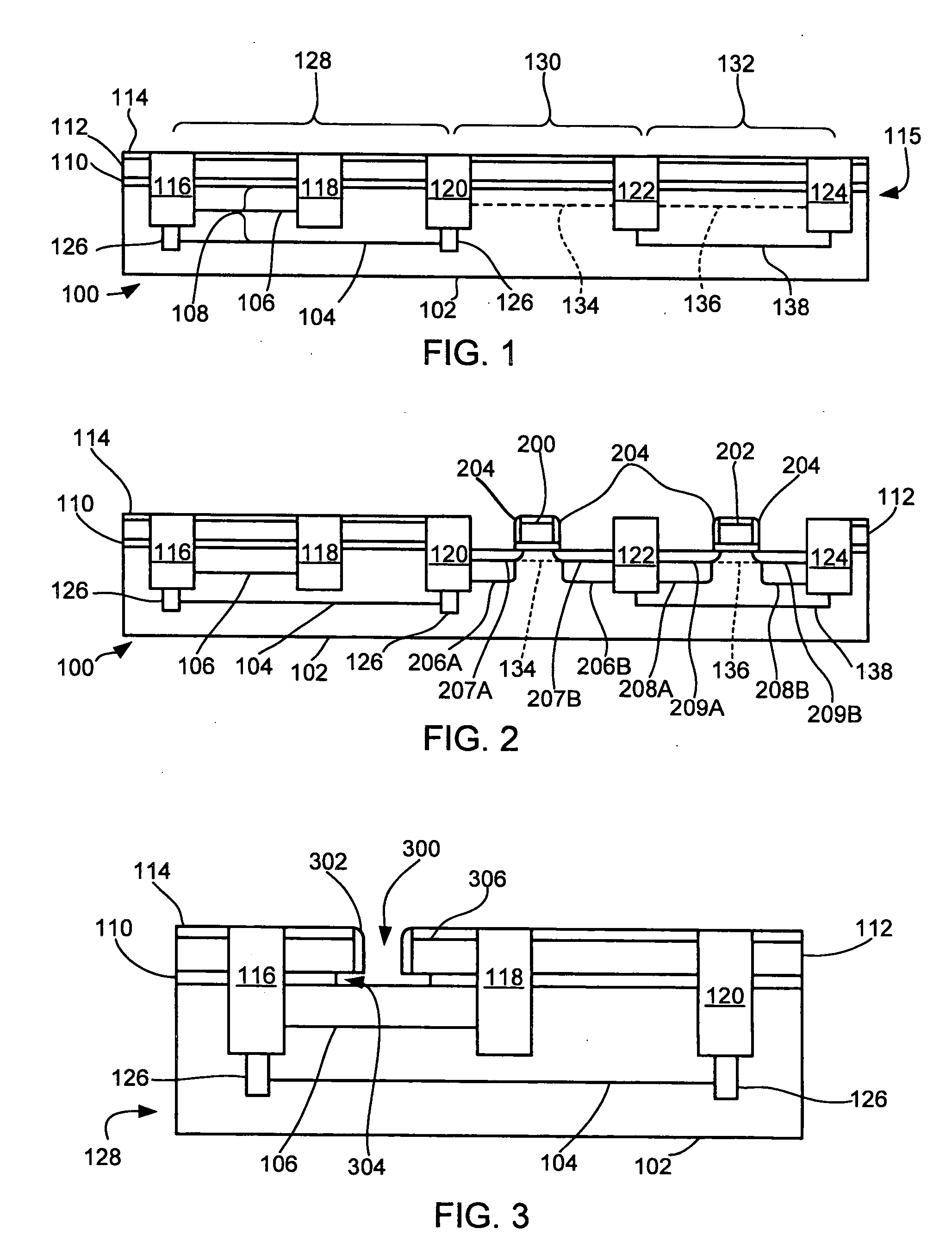
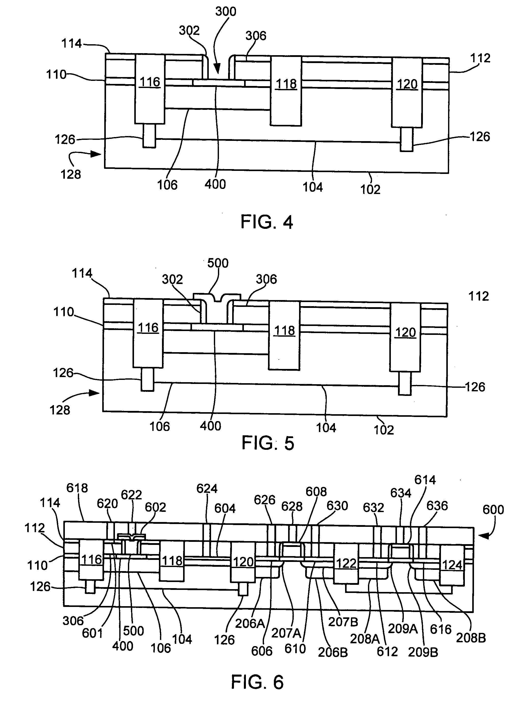
[0024] In the following description, numerous specific details are given to provide a thorough understanding of the invention. However, it will be apparent to one skilled in the art that the invention may be practiced without these specific details. In order to avoid obscuring the present invention, some well-known configurations and process steps are not disclosed in detail.

[0025] Likewise, the drawings showing embodiments of the apparatus are semi-diagrammatic and not to scale and, particularly, some of the dimensions are for the clarity of presentation and are shown greatly exaggerated in the FIGs. Generally, the device can be operated in any orientation.

[0026] The term “horizontal” as used herein is defined as a plane parallel to the conventional plane or surface of a semiconductor wafer or substrate, regardless of its orientation. The term “vertical” refers to a direction perpendicular to the horizontal as just defined. Terms, such as “on”, “above”, “below”, “bottom”, “top”, ...


PUM


Abstract

A method of manufacturing a BiCMOS integrated circuit including a CMOS transistor having a gate structure, and a heterojunction bipolar transistor having an extrinsic base structure. A substrate is provided, and a polysilicon layer is formed over the substrate. The gate structure and the extrinsic base structure are formed in the polysilicon layer. A plurality of contacts is formed through the interlevel dielectric layer to the CMOS transistor and the heterojunction bipolar transistor.

Description

TECHNICAL FIELD [0001] The present invention relates generally to semiconductor technology, and more particularly to a method and apparatus for manufacturing BiCMOS integrated circuits having a heterojunction bipolar transistor. BACKGROUND ART [0002] Transistors are multi-electrode semiconductor devices in which the current flowing between two specified electrodes is controlled or modulated by the voltage applied at a third (control) electrode. Transistors fall into two major classes: field-effect transistors (FETs), and bipolar junction transistors (BJTs). [0003] FETs include a source, a drain, and a gate. A voltage applied to the gate results in a current flow between the source and the drain of the FET through a channel that is formed beneath the gate. A commonly used FET is a complimentary metal oxide semiconductor (CMOS) transistor. CMOS transistors can be either NMOS or PMOS transistors depending upon the type of semiconductive materials used to form the transistor. NMOS trans...

Claims


Application Information

Patent Timeline
Patent Type & Authority Applications(United States)
IPC IPC(8): H01L21/331H01L21/8249H01L27/06
CPCH01L21/8249H01L29/66242H01L27/0623
Inventor CHAN, LAPZHENG, JIA ZHENVERMA, PURAKH RAJLI, JIAN XUNCHU, SHAO-FU SANFORD
Owner CHARTERED SEMICONDUCTOR MANUFACTURING
Why Eureka
Try Eureka