Semiconductor memory

a technology of memory and semiconductors, applied in the field of semiconductor memory, can solve the problems of insufficient reduction of access time, data retained in memory cells might be corrupted, and disadvantages of higher capacities, and achieve the effect of reducing power consumption and reducing power consumption of semiconductor memory

Inactive Publication Date: 2005-07-07
SOCIONEXT INC
View PDF2 Cites 10 Cited by
  • Summary
  • Abstract
  • Description
  • Claims
  • Application Information

AI Technical Summary

Benefits of technology

[0049] In the first operation mode, when the first or second short refresh operation is performed in response to the refresh request, the semiconductor memory attempts the normal refresh operation on the selected word line after this first or second refresh operation. The semiconductor memory enters the second operation mode when the access request has precedence and the normal refresh operation on the selected word line cannot be performed before the next refresh request occurs. Since the decision on the entry to the second operation mode is postponed for a predetermined period, whether the frequency of supply of the access request is temporarily high or remains high can be decided with reliability. It is therefore possible to enter an optimum operation mode in accordance with the access frequency. As a result, the per...

Problems solved by technology

The SRAMs are, however, greater than DRAMs in the number of devices for constituting each single bit of cell, and thus are disadvantageous for higher capacities.
Consequently,...

Method used


Image

  • Semiconductor memory
  • Semiconductor memory
  • Semiconductor memory

Examples


first embodiment

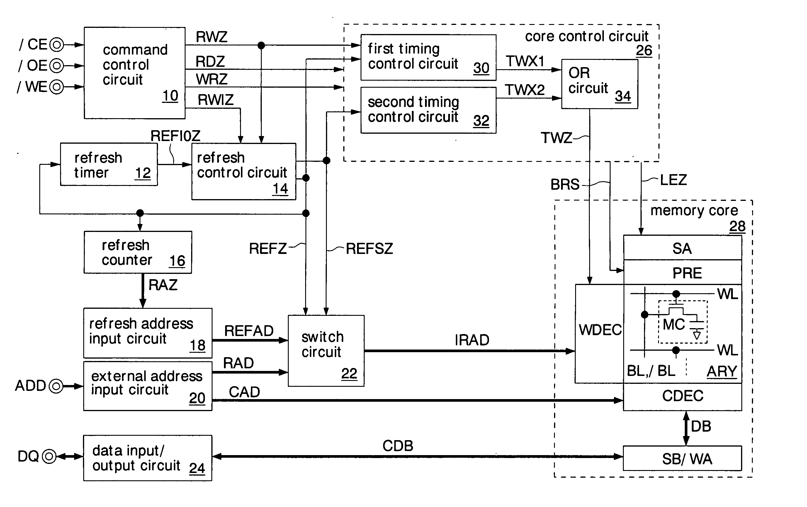
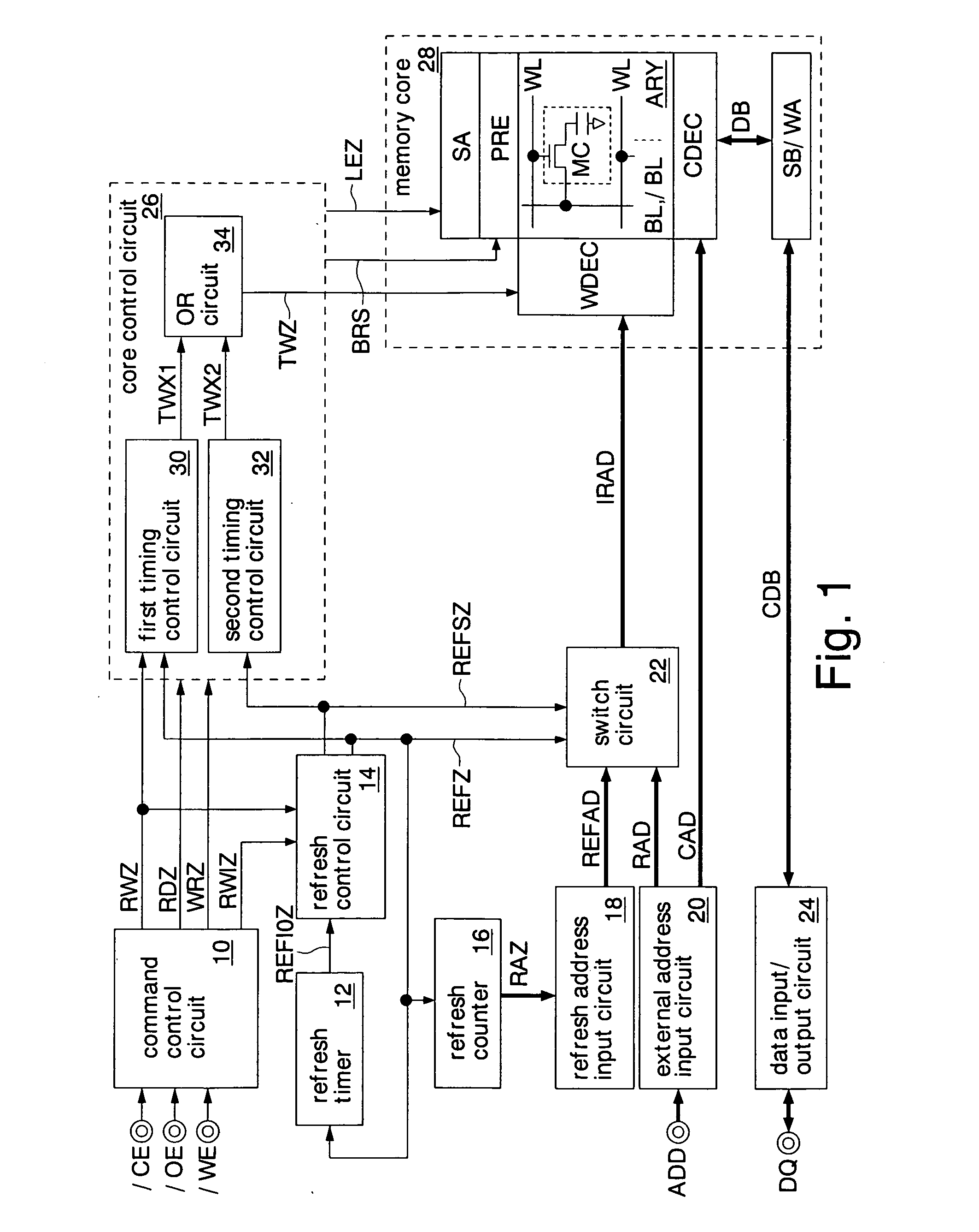
[0092]FIG. 1 shows the semiconductor memory of the present invention. This semiconductor memory is formed as a pseudo SRAM which has DRAM memory cells and an SRAM interface. The pseudo SRAM performs periodic refresh operations inside the chip without receiving refresh commands from exterior, thereby retaining data written in its memory cells. This pseudo SRAM is used, for example, as a work memory to be mounted on a cellular phone.

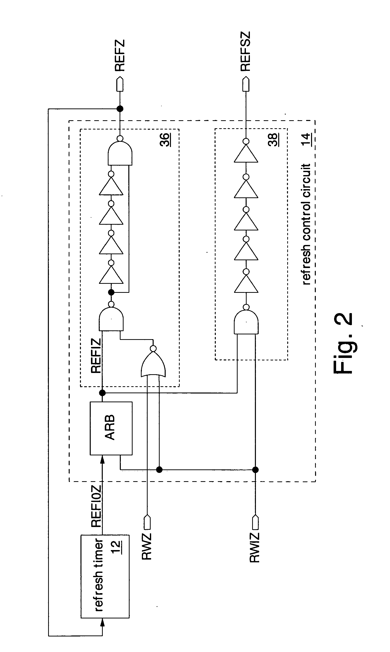
[0093] The pseudo SRAM has a command control circuit 10, a refresh timer 12, a refresh control circuit 14, a refresh counter 16, a refresh address input circuit 18, an external address input circuit 20, a switch circuit 22, a data input / output circuit 24, a core control circuit 26, and a memory core 28.

[0094] The command control circuit 10 receives command signals (a chip enable signal / CE, an output enable signal / OE, and a write enable signal / WE) from exterior through command terminals, decodes the received commands, and outputs a read control ...

second embodiment

[0167]FIG. 12 shows another operation of the pseudo SRAM according to the Detailed description will be omitted of the same operations as in FIGS. 6, 7, and 11 seen above.

[0168] In this example, two read operations RD are performed in succession, and the refresh request signal REFI0Z occurs after the supply of the first read command. The operations are the same as in the first embodiment (FIG. 7) except that the real refresh operation REFr is performed between the read operations RD.

[0169] As above, the second embodiment can provide the same effects as those of the first embodiment described above. Moreover, in this embodiment, the execution time of the normal refresh operation REF is shorter than the execution times of the write operation WR and the read operation RD. This produces a timing margin between the execution of the normal refresh operation and the execution of the next access operation RD or WR. Consequently, the core control circuit 26A and the like can be improved in ...

third embodiment

[0193]FIG. 17 shows another operation of the pseudo SRAM according to the Detailed description will be omitted of the same operations as in FIGS. 6 and 7 seen above.

[0194] In this example, as in the first embodiment (FIG. 7), two read operations RD are performed in succession, and the refresh request signal REFI0Z occurs after the supply of the first read command. Thus, the short refresh operation REF will not be performed. The late occurrence of the refresh request signal REFI0Z also delays the rising edge of the refresh request signal REFIX (FIG. 17(a)). Consequently, the refresh counter 16 counts up after the second read operation RD (FIG. 17(b)). The rest of the operations are the same as in FIG. 16 seen above.

[0195] The third embodiment can provide the same effects as those of the first embodiment described above.


PUM


Abstract

A refresh signal is output in response to a refresh request generated at predetermined cycles, and a refresh operation is performed. The refresh operation ends when a conflict occurs between an access request and the refresh request. Consequently, an access operation corresponding to the access request can be started earlier with a reduction in access time. The access time can be reduced further by changing the end time of the refresh operation in accordance with the timing of supply of the access request. Since a test circuit for notifying the state of the refresh operation to exterior is formed, the operation margin of the refresh operation can be evaluated in a short time. As a result, it is possible to reduce the development period of the semiconductor memory.

Description

CROSS REFERENCE TO RELATED APPLICATION [0001] This application is a continuation application of International Application PCT / JP 02 / 11555, filed on Nov. 6, 2002 and claims the benefit of priority from Japanese Patent Application No. 2002-274970, filed on Sep. 20, 2002, and designating the U.S.BACKGROUND OF THE INVENTION [0002] 1. Field of the Invention [0003] The present invention relates to a semiconductor memory which requires periodic refresh operations to retain data written in its memory cells. In particular, the present invention relates to a semiconductor memory which performs refresh operations automatically inside without requiring a refresh command from exterior. In addition, the present invention relates to a technology for testing the foregoing semiconductor memory. [0004] 2. Description of the Related Art [0005] In recent years, mobile apparatuses such as a cellular phone have become more sophisticated in service facilities, and the amounts of data to be handled have be...

Claims


Application Information

Patent Timeline
IPC IPC(8): G11C7/00G11C11/406G11C29/02
CPCG11C11/401G11C11/406G11C11/40603G11C29/02G11C2211/4061G11C29/50012G11C29/50016G11C2029/0403G11C29/028G11C11/4091
Inventor SHINOZAKI, NAOHARUKANDA, TATSUYASATO, TAKAHIKOFUNYU, AKIHIRO
Owner SOCIONEXT INC
Why Eureka
Try Eureka