Recording medium comprising ferroelectric layer, nonvolatile memory device comprising recording medium, and methods of writing and reading data for the memory device

a technology of ferroelectric layer and recording medium, which is applied in mechanical recording, nanoinformatics, instruments, etc., can solve the problems of difficult to sufficiently reduce the size of the memory device, difficult to enhance the integration degree of flash memory, and limit the size of the hard disk which is a conventional data, etc., to achieve simple reading process, enhance reading speed, and little or no abrasion of the ferroelectric layer

Inactive Publication Date: 2005-07-07
SAMSUNG ELECTRONICS CO LTD
View PDF7 Cites 27 Cited by
  • Summary
  • Abstract
  • Description
  • Claims
  • Application Information

AI Technical Summary

Benefits of technology

[0026] There is little or no abrasion of the ferroelectric layer because the probe does not directly contact the ferroelectric layer. Moreover, the method of reading data of the present invention can enhance reading speed since the reading process is simple, and thus, a highly enhanced storage capability is maintained. In addition, an extra device to write and read data is not required, thereby minimizing the size of the memory device.

Problems solved by technology

However, there are limitations in minimizing the size of a hard disk which is a conventional data storage device.
A flash memory could be used as an alternative to the hard disc, however, it is very difficult to enhance integration degree of the flash memory.
A memory device that senses a polarized state of a domain of the ferroelectric layer using piezoelectric force utilizes a lock-in amplifier, and thus, it is difficult to sufficiently reduce the size of the memory device.
The latter method, that is, the heating method, proceeds very slowly and is disadvantageous when the reading and writing processes are repeated.
Thus, it is difficult to minimize the size of the memory device for mobile products.
On the other hand, if the probe contacts the recording medium, while data is read, abrasion of the probe and-the recording medium, especially that of the recording medium, may be a serious problem.
In addition, data reading speed can be limited due to the resonance frequency of a cantilever (normally 1 MHz or less) which supports the probe.

Method used


Image

  • Recording medium comprising ferroelectric layer, nonvolatile memory device comprising recording medium, and methods of writing and reading data for the memory device
  • Recording medium comprising ferroelectric layer, nonvolatile memory device comprising recording medium, and methods of writing and reading data for the memory device
  • Recording medium comprising ferroelectric layer, nonvolatile memory device comprising recording medium, and methods of writing and reading data for the memory device

Examples


first embodiment

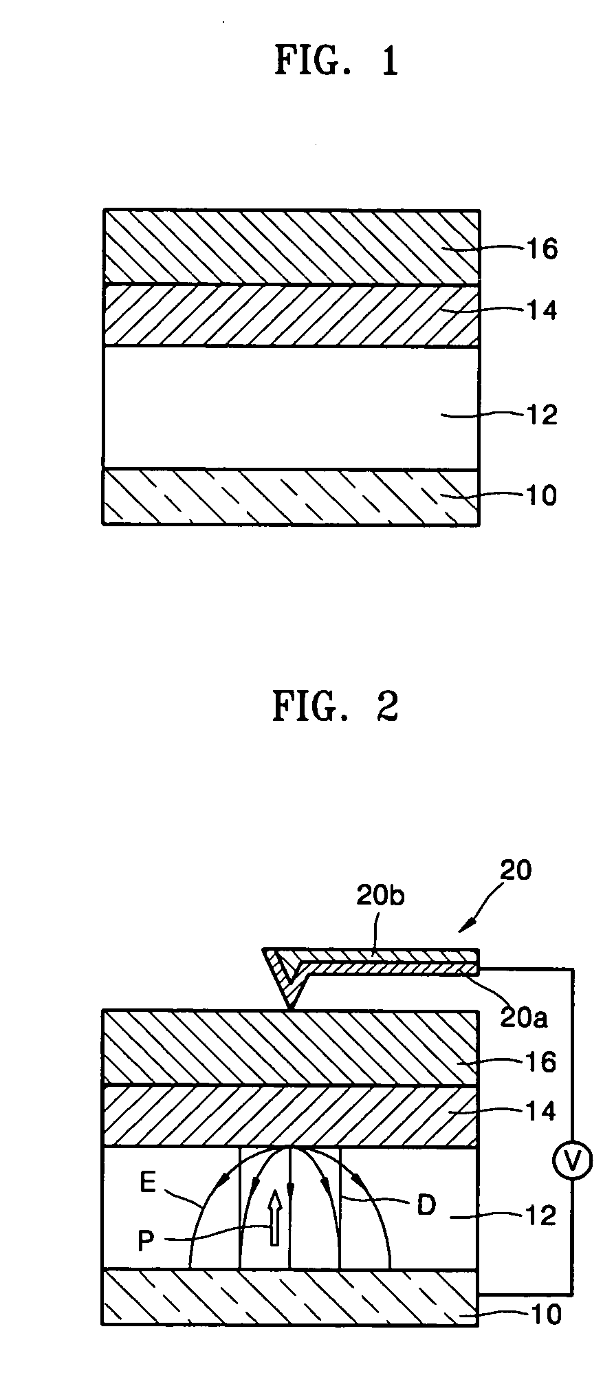
[0043]FIG. 1 is a cross-sectional view of a recording medium according to the present invention.

[0044] Referring to FIG. 1, the recording medium according to a first embodiment of the present invention includes a lower electrode 10 to which a predetermined voltage is applied when data is written, a ferroelectric layer 12, in which the data is written, a first semiconductor layer 16 to which the predetermined voltage is applied when the data that is written in the ferroelectric layer 12 is read, and a barrier layer 14 disposed between the ferroelectric layer 12 and the first semiconductor layer 16. The barrier layer 14 prevents reactions between the first semiconductor layer 16 and the ferroelectric layer 12 during fabrication and also serves as a gate oxide layer. Preferably, but not necessarily, the ferroelectric layer 12 is composed of a material having strong vertical polarization characteristics. In addition, the ferroelectric layer 12 may be a first ferroelectric layer which ha...

second embodiment

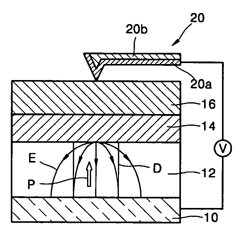
[0049] Referring to FIG. 2, the probe 20 contacts the first semiconductor layer 16 and writes data in the recording medium according to the present invention. The probe 20 includes a first portion 20a that contacts the surface of the first semiconductor layer 16 and a second portion 20b that supports the first portion 20a. The first portion 20a is preferably formed of Pt, but any metal that forms a Schottkey junction with the first semiconductor layer 16 can be used. For example, the first portion 20a may be formed of Au and the second portion 20b may be formed of a silicon (Si) layer or a silicon nitride layer (Si3N4).

[0050] The method of writing data in the recording medium using the probe 20 will now be described in detail.

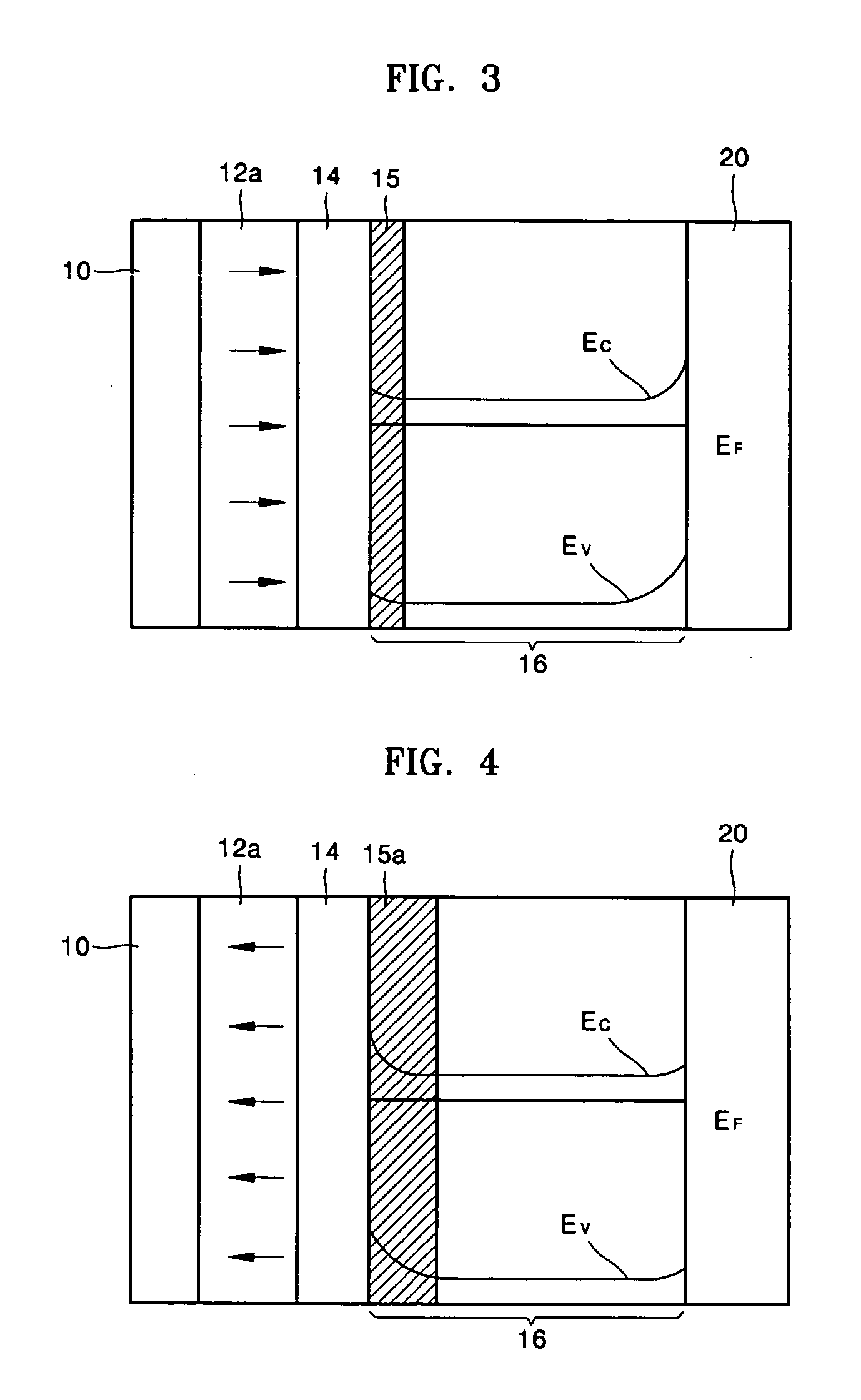
[0051] First, a voltage is applied between the probe 20 and the lower electrode 10, while the probe 20 contacts the surface of the first semiconductor layer 16. An electric field E appears between the probe 20 and the lower electrode 10. The probe 20 contacts ...


PUM

PropertyMeasurementUnit
resonance frequencyaaaaaaaaaa
thicknessaaaaaaaaaa
gate voltage Vgaaaaaaaaaa

Abstract

A recording medium including a ferroelectric layer, a nonvolatile memory device including the recording medium and methods of wiring and reading data in the memory device. The recording medium includes: a lower electrode; a ferroelectric layer to which data is recorded, formed on the lower electrode; a barrier layer formed on the ferroelectric layer; and a semiconductor layer formed on the barrier layer. The nonvolatile memory device includes a probe that reads and writes the data. Furthermore, in the method of writing data, a writing voltage is applied between the probe, which contacts the semiconductor layer, and the lower electrode and, in the method of reading data, a state of a remanent polarization of the ferroelectric layer is determined by applying a reading voltage between the probe and the semiconductor layer.

Description

BACKGROUND OF THE INVENTION [0001] This application claims the priority of Korean Patent Application Nos. 2003-58790, filed on Aug. 25, 2003, and 2004-2925, filed on Jan. 15, 2004, in the Korean Intellectual Property Office, the disclosure of which is incorporated herein in its entirety by reference. [0002] 1. Field of the Invention [0003] The present invention relates to a recording medium, a memory device including the recording medium, and methods of writing and reading data for the memory device, and more particularly, to a recording medium including a ferroelectric layer, a nonvolatile memory device including the recording medium, and methods of writing and reading data for the nonvolatile memory device. [0004] 2. Description of the Related Art [0005] As the demand for small and thin electronic devices such as mobile telecommunication devices and electronic notes increases, the necessity of ultra-small and integrated memory devices also increases. However, there are limitations...

Claims


Application Information

Patent Timeline
Patent Type & Authority Applications(United States)
IPC IPC(8): G11B9/00G11B9/02G11B9/14G11C11/22
CPCB82Y10/00G11B9/02G11B9/14G11C11/22G11B9/1463G11B9/1472G11B9/1409
Inventor KIM, YUN-SEOKHONG, SEUNG-BUMNO, KWANG-SOO
Owner SAMSUNG ELECTRONICS CO LTD
Why Eureka
Try Eureka