Recording medium comprising ferroelectric layer, nonvolatile memory device comprising recording medium, and methods of writing and reading data for the memory device
a technology of ferroelectric layer and recording medium, which is applied in mechanical recording, nanoinformatics, instruments, etc., can solve the problems of difficult to sufficiently reduce the size of the memory device, difficult to enhance the integration degree of flash memory, and limit the size of the hard disk which is a conventional data, etc., to achieve simple reading process, enhance reading speed, and little or no abrasion of the ferroelectric layer
- Summary
- Abstract
- Description
- Claims
- Application Information
AI Technical Summary
Benefits of technology
Problems solved by technology
Method used
Image
Examples
first embodiment
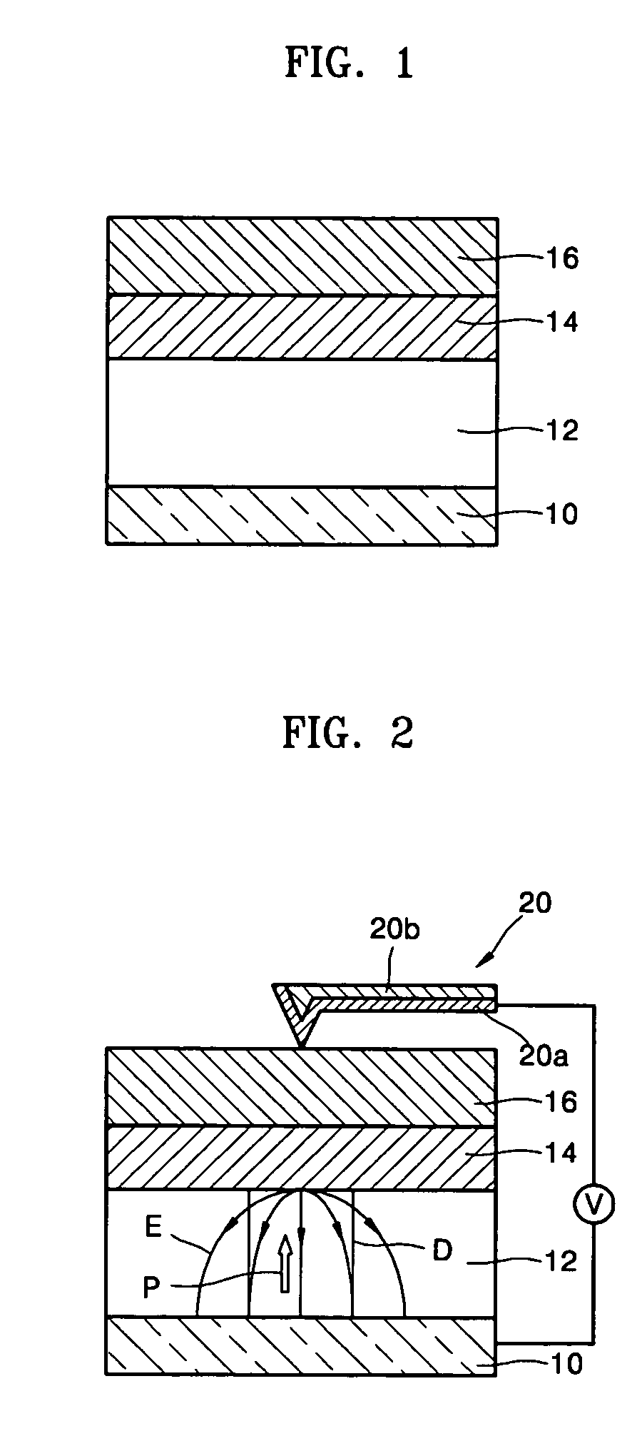
[0043]FIG. 1 is a cross-sectional view of a recording medium according to the present invention.
[0044]Referring to FIG. 1, the recording medium according to a first embodiment of the present invention includes a lower electrode 10 to which a predetermined voltage is applied when data is written, a ferroelectric layer 12, in which the data is written, a first semiconductor layer 16 to which the predetermined voltage is applied when the data that is written in the ferroelectric layer 12 is read, and a barrier layer 14 disposed between the ferroelectric layer 12 and the first semiconductor layer 16. The barrier layer 14 prevents reactions between the first semiconductor layer 16 and the ferroelectric layer 12 during fabrication and also serves as a gate oxide layer. Preferably, but not necessarily, the ferroelectric layer 12 is composed of a material having strong vertical polarization characteristics. In addition, the ferroelectric layer 12 may be a first ferroelectric layer which has...
second embodiment
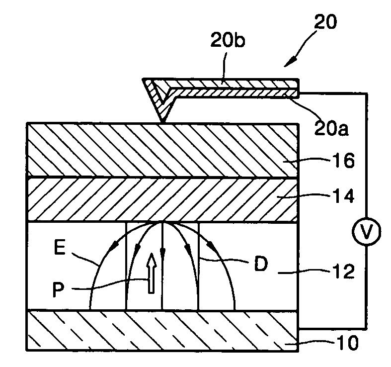
[0049]Referring to FIG. 2, the probe 20 contacts the first semiconductor layer 16 and writes data in the recording medium according to the present invention. The probe 20 includes a first portion 20a that contacts the surface of the first semiconductor layer 16 and a second portion 20b that supports the first portion 20a. The first portion 20a is preferably formed of Pt, but any metal that forms a Schottkey junction with the first semiconductor layer 16 can be used. For example, the first portion 20a may be formed of Au and the second portion 20b may be formed of a silicon (Si) layer or a silicon nitride layer (Si3N4).
[0050]The method of writing data in the recording medium using the probe 20 will now be described in detail.
[0051]First, a voltage is applied between the probe 20 and the lower electrode 10, while the probe 20 contacts the surface of the first semiconductor layer 16. An electric field E appears between the probe 20 and the lower electrode 10. The probe 20 contacts the ...
PUM
| Property | Measurement | Unit |
|---|---|---|
| resonance frequency | aaaaa | aaaaa |
| thickness | aaaaa | aaaaa |
| gate voltage Vg | aaaaa | aaaaa |
Abstract
Description
Claims
Application Information


