
Process for producing light-emitting semiconductor device

a technology of semiconductor devices and semiconductor elements, applied in the direction of coatings, optical articles, other domestic articles, etc., can solve the problems of damage to light-emitting semiconductor elements, troublesome steps, cost, etc., and achieve the effect of satisfying the efficiency of light takeou

Inactive Publication Date: 2005-07-07
NITTO DENKO CORP
View PDF11 Cites 12 Cited by
  • Summary
  • Abstract
  • Description
  • Claims
  • Application Information

AI Technical Summary

Benefits of technology

[0011] 1. A process for producing a light-emitting semiconductor device which comprises:
[0012] (1) forming a polycarbodiimide-containing layer on a light takeout side of a light-emitting semiconductor element; and
[0013] (2) forming irregularities on the surface of the polycarbodiimide-containing layer.
[0014] 2. The process for producing a light-emitting semiconductor device of item 1 above, wherein the polycarbodiimide-containing layer contains a polycarbodiimide represented by general formula (1): R1—N═C═NR—N═C═NnR1   (1) wherein R represents a diisocyanate residue, R1 represents a monoisocyanate reside, and n is an integer of 1 to 100.
[0015] 3. The process for producing a light-emitting semiconductor device of item 1 or 2 above, wherein the polycarbodiimide-containing layer before the formation of irregularities has a thickness of 0.5 to 10 μm.
[0016] According to the inventions the light-emitting semiconductor element can be prevented from being damaged during production and a light-emitting semiconductor device having a satisfactory efficiency of light takeout can be produced.

Problems solved by technology

However, the processing of a semiconductor surface for forming irregularities thereon necessitates etching by the RIE (reactive ion etching) or ion milling method and this step takes troubles and costs.
However, since the film comprises a polyimide, the formation of irregularities on the surface of the film with a die press usually necessitates application of a pressure higher than 1 MPa to the light-emitting semiconductor element at 300° C. or higher.
There is a possibility that such a high temperature and high pressure might damage the light-emitting semiconductor element.

Method used


Image

  • Process for producing light-emitting semiconductor device
  • Process for producing light-emitting semiconductor device

Examples


production example 1

Production of Polycarbodiimide:

[0078] Into a 500-mL four-necked flask equipped with a stirrer, dropping funnel, reflux condenser, and thermometer were introduced 29.89 g (171.6 mmol) of tolylene diisocyanate (isomer mixture; T-80, manufactured by Mitsui-Takeda Chemical), 94.48 g (377.52 mmol) of 4,4′-diphenylmethane diisocyanate, 64.92 g (308.88 mmol) of naphthalene diisocyanate, and 184.59 g of toluene. These ingredients were mixed together.

[0079] Thereto were added 8.71 g (51.48 mmol) of 1-naphthyl isocyanate and 0.82 g (4.29 mmol) of 3-methyl-1-phenyl-2-phospholene 2-oxide. The resultant mixture was heated to 100° C. with stirring and held for 2 hours.

[0080] The end point of the reactions was ascertained by IR analysis and the reaction mixture was cooled to room temperature. Thus, a polycarbodiimide solution was obtained. In this polycarbodiimide, 100% by mole of the diisocyanate residues were aromatic diisocyanate residues. This polycarbodiimide was represented-by formula (1...

production example 2

Production of Polycarbodiimide Sheet:

[0083] The polycarbodiimide solution obtained in Production Example 1 was applied to a separator (thickness, 50 μm) (manufactured by Toray Industries, Inc.) made of poly(ethylene terephthalate) treated with a release agent (fluorinated silicone). The solution applied was heated at 130° C. for 1 minute and then heated at 150° C. for 1 minute. The separator was removed to obtain a temporarily cured sheet-form polycarbodiimide (thickness, 20 μm).

example 1

Production of Light-Emitting Semiconductor Devices:

[0084] An element (diameter, 100 mm; thickness, 100 μm) was prepared which had been obtained by forming a GaN layer on a sapphire substrate and forming an electrode (gold electrode) on the GaN layer.

[0085] The coating fluid produced in Production Example 1 was applied on the surface of the element by spin coating (5,000 rpm; 60 seconds) and dried at 120° C. for 30 minutes with a non-circulating drying oven to form a polycarbodiimide layer having a thickness of 2 μm.

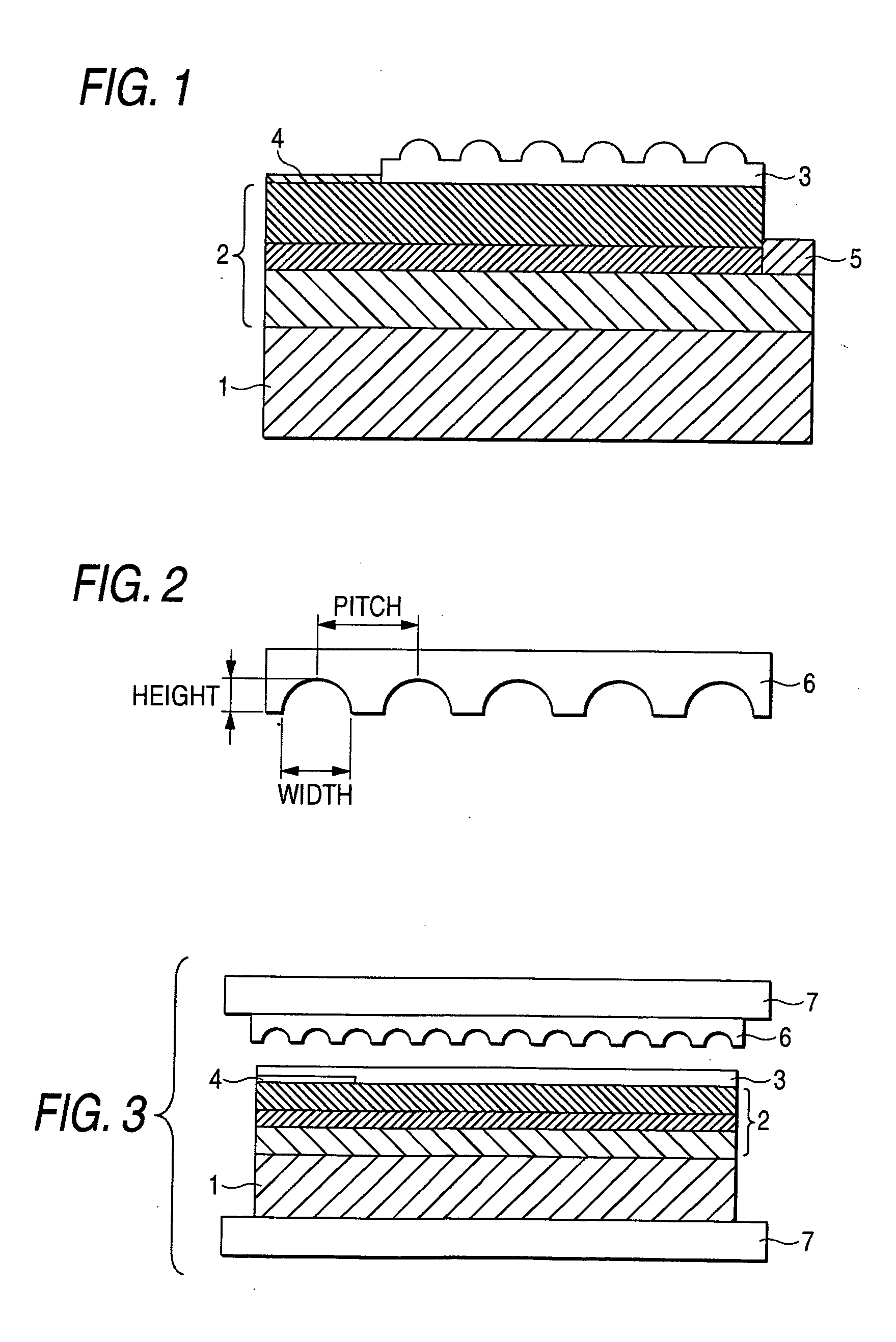
[0086] Subsequently, a die made of nickel (110 mm×110 mm) was prepared which had semispherical recesses each having a width of 4 μm and a height of 2 μm at a pitch of 6 μm as shown in FIG. 2.

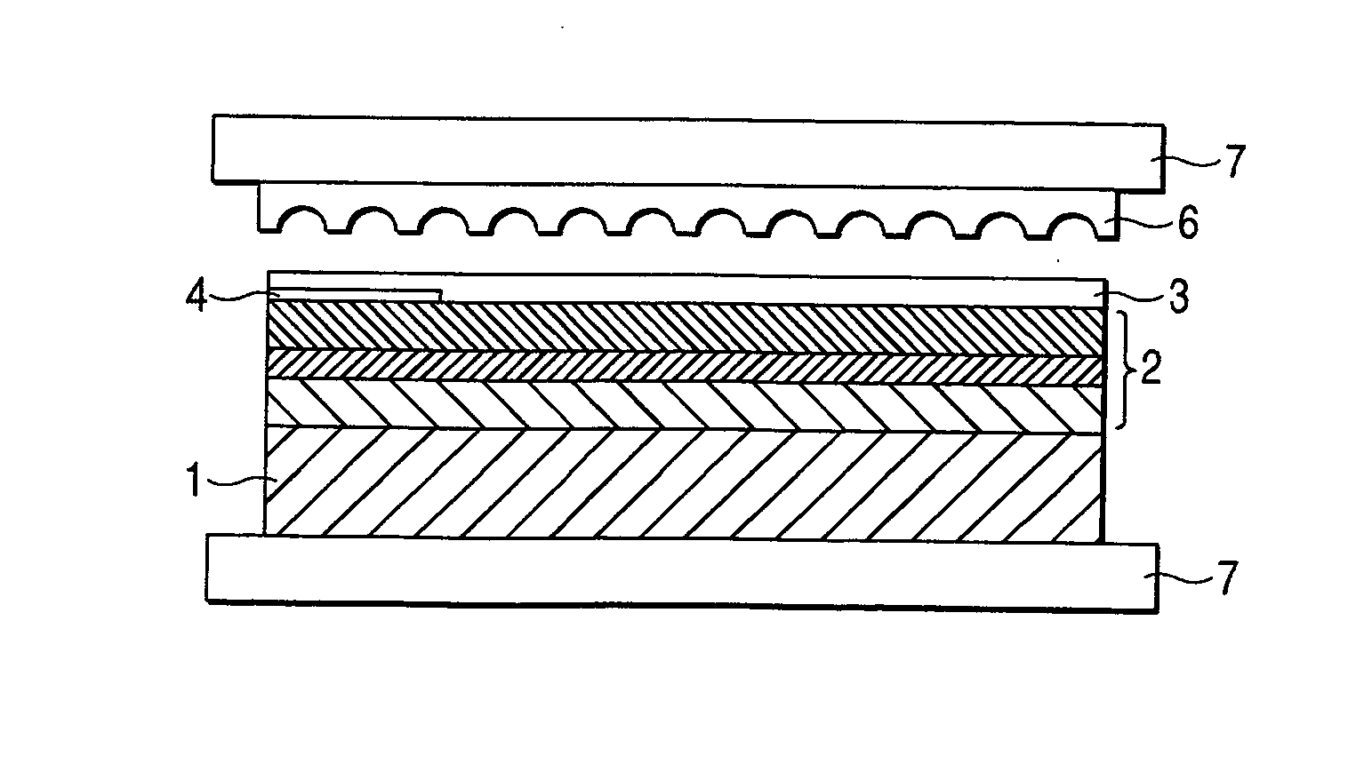
[0087] The die 6 and the light-emitting semiconductor element having thereon the polycarbodiimide layer were set between the heated pressing plates 7 of a pressing type vacuum laminator (V130, manufactured by Nichigo-Morton Co., Ltd.) as shown in FIG. 3. The element having the po...


PUM

PropertyMeasurementUnit
thicknessaaaaaaaaaa
refractive indexaaaaaaaaaa
heightaaaaaaaaaa

Abstract

The invention provides a process for producing a light-emitting semiconductor device, which comprises: (1) forming a polycarbodiimide-containing layer on a light takeout side of a light-emitting semiconductor element; and (2) forming irregularities on the surface of the polycarbodiimide-containing layer.

Description

FIELD OF THE INVENTION [0001] The present invention relates to a process for producing a light-emitting semiconductor device. BACKGROUND OF THE INVENTION [0002] There has been reported a technique in which irregularities are formed on the light takeout surface of a light-emitting semiconductor element in order to heighten the efficiency in light takeout of the light-emitting semiconductor element (see, for example, patent document 1). [0003] However, the processing of a semiconductor surface for forming irregularities thereon necessitates etching by the RIE (reactive ion etching) or ion milling method and this step takes troubles and costs. [0004] Hence, there has been proposed a technique in which an antireflection film comprising a polyimide resin and TiO2 added thereto is formed on the light takeout surface of a light-emitting semiconductor element and irregularities are formed on the surface of the film with a die press to thereby improve the efficiency in light takeout (see, fo...

Claims


Application Information

Patent Timeline
Patent Type & Authority Applications(United States)
IPC IPC(8): B29C43/02B29C43/20C08G18/02C08G18/71C08G18/76C09D175/00H01L21/00H01L29/06H01L31/0328H01L31/0336H01L31/072H01L31/109H01L33/44
CPCB29C43/021B29C43/203B29L2011/00B29L2011/0016H01L2933/0091C08G18/71C08G18/7607C09D175/00H01L33/44C08G18/025
Inventor SUEHIRO, ICHIROUHOTTA, YUJISADAYORI, NAOKIHARADA, NORIAKI
Owner NITTO DENKO CORP
Learn More