
Crystallization apparatus, optical member for use in crystallization apparatus, crystallization method, manufacturing method of thin film transistor, and manufacturing method of matrix circuit substrate of display

Inactive Publication Date: 2006-09-05
ADVANCED LCD TECH DEVMENT CENT
View PDF12 Cites 40 Cited by
  • Summary
  • Abstract
  • Description
  • Claims
  • Application Information

AI Technical Summary

Benefits of technology

[0013]An object of the present invention is to provide a crystallization apparatus and method in which a large part of light supplied from an optical illumination system can contribute to crystallization of a desired region and in which light efficiency is satisfactory.
[0014]Another object of the present invention is to provide a crystallization apparatus and method in which sufficient lateral growth from a crystal nucleus can be realized to produce a crystallized semiconductor film having a large grain diameter.
[0015]Further object of the present invention is to provide a manufacturing method of a thin film transistor having an effect similar to the above-described effect, and a manufacturing method of a matrix circuit substrate of a display.

Problems solved by technology

Moreover, in the thin film transistor (FET) formed using the poly silicon, fluctuation of the number of crystal grain boundaries existing in a channel portion is a problem.
Therefore, a large part of the laser beam supplied from an optical illumination system does not contribute to the crystallization of the transistor forming region, and a so-called light amount loss is very large.
However, it is impossible to control the light intensity distribution in an intermediate portion between two inverse peak portions disposed opposite to each other.
In this case, in a process of crystallization, the lateral growth started toward the periphery from the crystal nucleus stops in a portion in which the light intensity decreases in the intermediate portion, and there is a problem that the growth of large crystals is inhibited.
Moreover, even if a substantially uniform light intensity distribution is obtained in the intermediate portion, the lateral growth stops in an arbitrary position in this uniform light intensity distribution, and there is a problem that the growth of large crystals is inhibited.

Method used


Image

  • Crystallization apparatus, optical member for use in crystallization apparatus, crystallization method, manufacturing method of thin film transistor, and manufacturing method of matrix circuit substrate of display
  • Crystallization apparatus, optical member for use in crystallization apparatus, crystallization method, manufacturing method of thin film transistor, and manufacturing method of matrix circuit substrate of display
  • Crystallization apparatus, optical member for use in crystallization apparatus, crystallization method, manufacturing method of thin film transistor, and manufacturing method of matrix circuit substrate of display

Examples


first embodiment

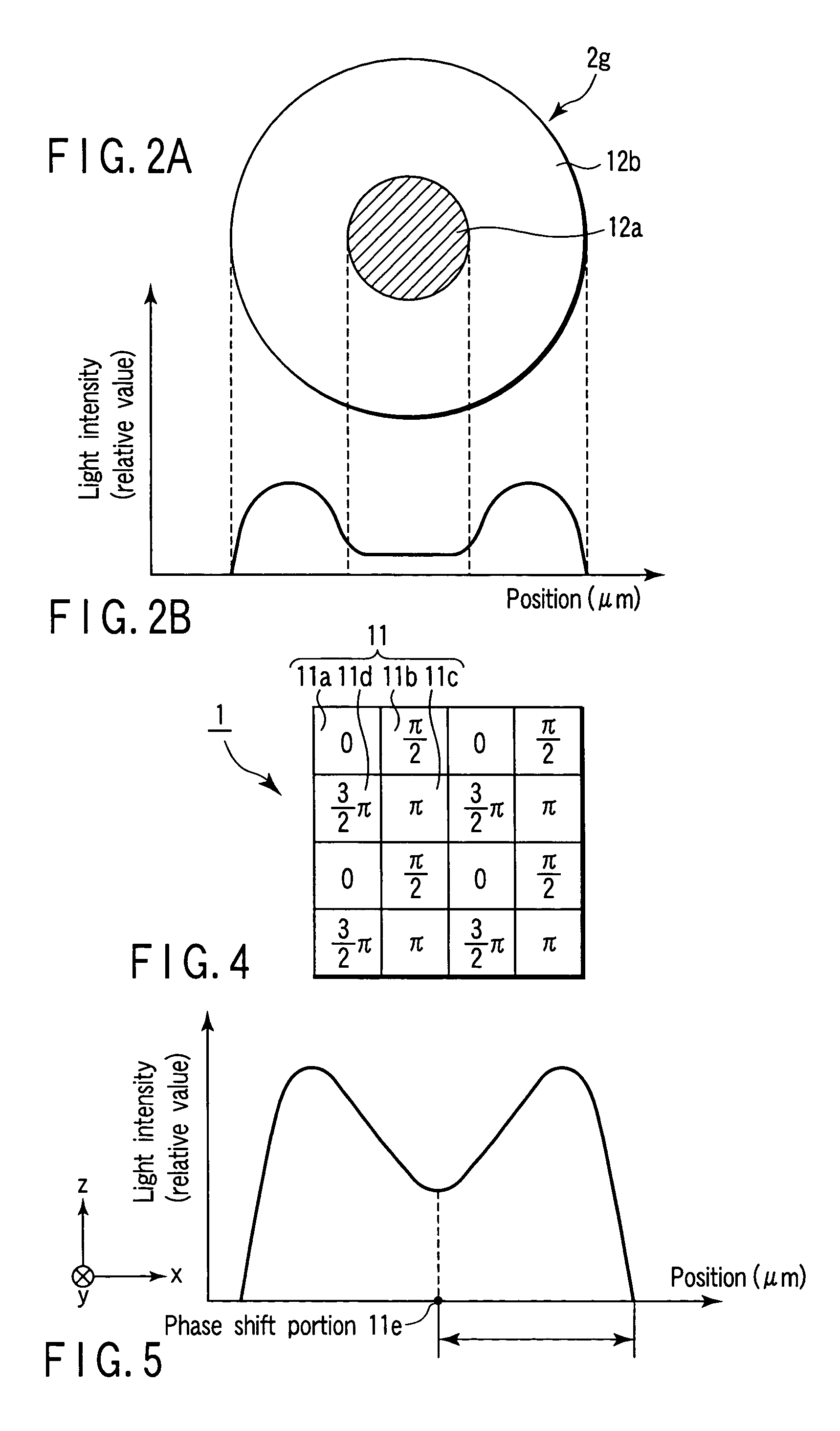
[0055]When the multilayered film is used as a reflective material, there is an advantage that heat is not generated by absorption of any unnecessary light. However, it needs to be considered that a reflected light should not form a stray light to cause flare. Types and thicknesses of the shield and reflective materials are preferably adjusted so that a phase difference is not substantially generated in the transmitted light in a boundary line between the middle region 12a and peripheral region 12b. In the first embodiment, an example of the middle region 12a which is formed in a circular shape has been described, but other shapes such as triangular and rectangular shapes may also be formed.

[0056]FIG. 3A is a perspective view schematically showing one of a large number of basic unit portions constituting the phase shift mask 1 in association with one of a large number of basic unit portions consisting of a convergence / divergence device including the micro lens array 3, that is, a wav...

second embodiment

[0083]In the second embodiment, the substrate to be treated 4 is distant from a plane optically conjugated with the phase shift mask 1 (image plane of the optical image forming system 6) along the optical axis. In this case, the width of the inverse peak type light intensity distribution of the laser beam formed into an image on the semiconductor film of the substrate to be treated 4 by the function of the phase shift mask 1 changes substantially in proportion to ½ square of the distance between the image plane of the optical image forming system 6 and the substrate to be treated 4 (i.e., a defocus amount), assuming that the resolution of the optical image forming system 6 is sufficient. It is to be noted that the optical image forming system 6 may be any of refractive, reflective and refractive / reflective optical systems.

[0084]Also in the second embodiment, in the same manner as in the first embodiment, the semiconductor film of the substrate to be treated 4 is irradiated with the ...

third embodiment

[0088]The optical image forming system 7 includes an aperture diaphragm 7a. The aperture diaphragm 7a is selected from a plurality of aperture diaphragms different in the size of an aperture (light transmission portion). These aperture diaphragms are constituted so that the diaphragms can selectively be converted with respect to the light path. Instead, the aperture diaphragm 7a may also be constituted such that the size of the aperture continuously changes, for example by moving the diaphragm. The size of the aperture of the aperture diaphragm 7a (i.e., the image-side numerical aperture of the optical image forming system 7) is set such that the light beam can include the periodic two-steps inverse peak type light intensity distribution on the semiconductor film of the substrate to be treated 4. The width of the two-steps inverse peak type light intensity distribution is preferably set to be equal to the pixel pitch of a liquid crystal display.

[0089]By the function of the phase sh...


PUM


Abstract

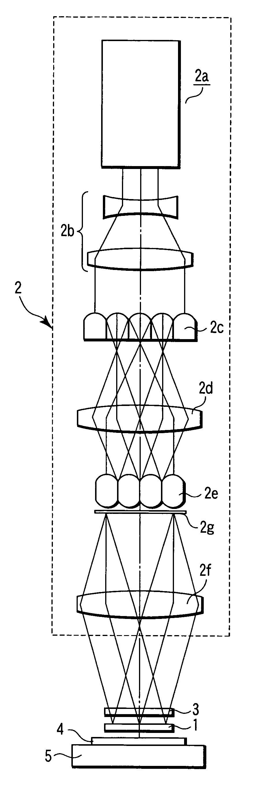
A crystallization apparatus includes an optical illumination system to illuminate a phase shift mask and which irradiates an amorphous semiconductor film with a light beam having an inverse peak type light intensity distribution including a minimum light intensity in a point corresponding to a phase shift portion of the phase shift mask to produce a crystallized semiconductor film. A wavefront dividing element is disposed on a light path between the optical illumination system and the phase shift mask. The wavefront dividing element wavefront-divides the light beam supplied from the optical illumination system into a plurality of light beams, and condenses the wavefront-divided light beams in the corresponding phase shift portion or in the vicinity of the portion.

Description

CROSS-REFERENCE TO RELATED APPLICATIONS[0001]This application is based upon and claims the benefit of priority from the prior Japanese Patent Application No. 2002-188846, filed Jun. 28, 2002, the entire contents of which are incorporated herein by reference.BACKGROUND OF THE INVENTION[0002]1. Field of the Invention[0003]The present invention relates to a crystallization apparatus for irradiating an amorphous or polycrystalline semiconductor film with a laser beam to produce a crystallized semiconductor film, an optical member for use in the crystallization apparatus, a crystallization method, a thin film transistor, and a display apparatus. The present invention particularly relates to an apparatus and method in which an amorphous or polycrystalline semiconductor film is irradiated with a laser beam phase-modulated using a phase shift mask to produce a crystallized semiconductor film.[0004]2. Description of the Related Art[0005]A material of a thin film transistor (TFT) for use in a...

Claims


Application Information

Patent Timeline
IPC IPC(8): C30B29/16G03B21/56H01L21/20H01L21/027H01L21/268
CPCG03B21/56Y10T117/1012Y10T117/1008Y10T117/1004Y10T117/10H01L21/027
Inventor TANIGUCHI, YUKIOMATSUMURA, MASAKIYOYAMAGUCHI, HIROTAKANISHITANI, MIKIHIKOTSUJIKAWA, SUSUMUKIMURA, YOSHINOBUJYUMONJI, MASAYUKI
Owner ADVANCED LCD TECH DEVMENT CENT
Learn More