Nitride semiconductor laser device and method for fabrication thereof

a laser device and semiconductor technology, applied in the direction of lasers, semiconductor laser structural details, semiconductor lasers, etc., can solve the problems of difficult fabrication of nitride semiconductor light-emitting devices, and achieve the effects of reducing film thickness, preventing cracks, and good surface flatness

Inactive Publication Date: 2005-07-14
SHARP KK
View PDF3 Cites 54 Cited by
  • Summary
  • Abstract
  • Description
  • Claims
  • Application Information

AI Technical Summary

Benefits of technology

[0043] The present invention has been devised to solve the conventionally encountered problems discussed above. It is, therefore, an object of the present invention to prevent cracks that develop in a nitride semiconductor growth layer when it is laid on top of a nitride semiconductor substrate to produce a nitride semiconductor laser device. It is another object of the present invention to prov...

Problems solved by technology

The reason is that, with an etching angle θ larger than 140°, it i...

Method used


Image

  • Nitride semiconductor laser device and method for fabrication thereof
  • Nitride semiconductor laser device and method for fabrication thereof
  • Nitride semiconductor laser device and method for fabrication thereof

Examples


Embodiment Construction

[0064] Hereinafter, embodiments of the present invention will be described with reference to the accompanying drawings.

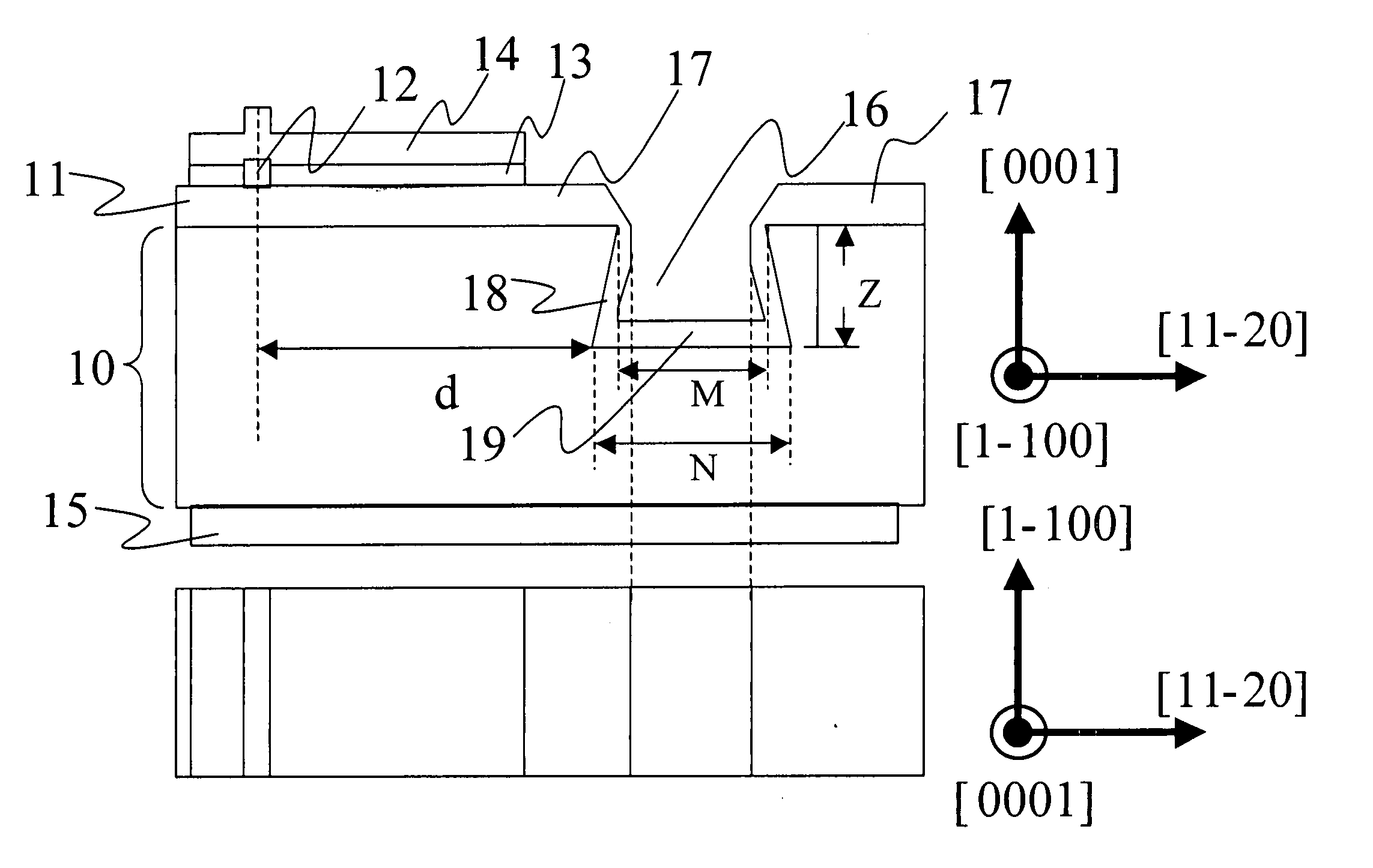
[0065]FIG. 1A is a schematic sectional view of a nitride semiconductor laser device embodying the invention, and FIG. 1B is a top view of FIG. 1A. FIG. 3B is a schematic sectional view of a GaN substrate before a nitride semiconductor layer is grown on top thereof in the embodiment of the invention, and FIG. 3A is a top view of FIG. 3B. In these diagrams, the surface orientations are also indicated.

[0066] The nitride semiconductor laser device shown in FIGS. 1A and 1B is produced by laying or otherwise forming a nitride semiconductor growth layer on top of the GaN substrate shown in FIGS. 3A and 3B.

[0067] In the following descriptions, a “nitride semiconductor substrate” is formed from AlxGayInzN (where 0≦x≦1, 0≦y≦1, 0≦z≦1, and x+y+z=1). So long as the nitride semiconductor substrate has a hexagonal crystal structure, about 10% or less of the nitrogen contained t...


PUM


Abstract

In a nitride semiconductor light-emitting device, and according to a method for fabricating it, a low-defect region having a defect density of 106 cm−2 or less and a carved region in the shape of a depressed portion are formed on the surface of a nitride semiconductor substrate, and the etching angle θ, which is the angle between the side surface portion of the depressed portion and an extension line of the bottom surface portion thereof as measured with the depressed portion seen in a sectional view, is in a range of 75°≦θ≦140°. This prevents the development of cracks, and reduces the creep-up growth from the bottom growth portion of the carved region, thereby reducing the film thickness of the side growth portion. This makes it possible to produce, with a high yield, a nitride semiconductor laser device having a nitride semiconductor growth layer with good surface flatness.

Description

[0001] This nonprovisional application claims priority under 35 U.S.C. § 119(a) on Patent Application No. 2004-000328 filed in Japan on Jan. 5, 2004, the entire contents of which are hereby incorporated by reference. BACKGROUND OF THE INVENTION [0002] 1. Field of the Invention [0003] The present invention relates to a nitride semiconductor laser device, and to a method for fabricating a nitride semiconductor laser device. More particularly, the present invention relates to a nitride semiconductor laser device that uses as the substrate thereof a nitride semiconductor. [0004] 2. Description of Related Art [0005] One feature of nitride semiconductors, for example GaN, AlGaN, GaInN, and AlGaInN, is that they have higher band gap energies than AlGaInAs-based and AlGaInP-based semiconductors. Another feature of such nitride semiconductors is that they are direct-transition semiconductor materials. [0006] Having these features, nitride semiconductors have recently been receiving much atte...

Claims


Application Information

Patent Timeline
IPC IPC(8): H01S5/343H01L29/22H01S5/02H01S5/323
CPCH01L33/20H01L33/32H01S2304/12H01S5/3202H01S5/32341H01S5/0207H01S5/2201H01S2301/176H01S5/320225H01S5/32025
Inventor KAMIKAWA, TAKESHIKANEKO, YOSHIKA
Owner SHARP KK
Why Eureka
Try Eureka