Output driver for use in semiconductor device

Active Publication Date: 2005-07-14
SAMSUNG ELECTRONICS CO LTD
View PDF12 Cites 5 Cited by
  • Summary
  • Abstract
  • Description
  • Claims
  • Application Information

AI Technical Summary

Benefits of technology

[0012] A feature of the present invention, therefore, is to provide an output driver for use in a semiconductor device capable of remarkably reducing an impedance change for outp

Problems solved by technology

However, as the swing width of the signal is reduced, an effect due to an external noise increases and reflection of an output signal due to impedance mismatching in an interface stage becomes critical.
The impedance mismatching is caused by an external noise or a change of power supply voltage, a change of operating temperature, a change of manufacturing process, or the like.
Occurrence of impedance mismatching makes high-speed data transmission difficult and may distort a signal outputted from a data output terminal of, the semiconductor device, namely, output data.
Accordingly, if a semiconductor device

Method used


Image

  • Output driver for use in semiconductor device
  • Output driver for use in semiconductor device
  • Output driver for use in semiconductor device

Examples


Embodiment Construction

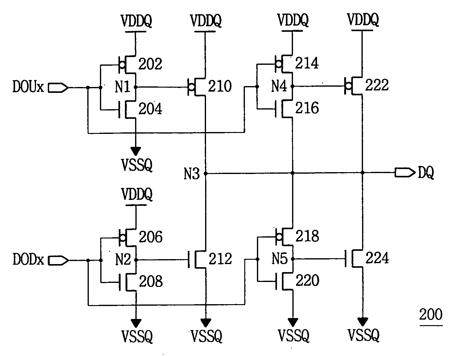
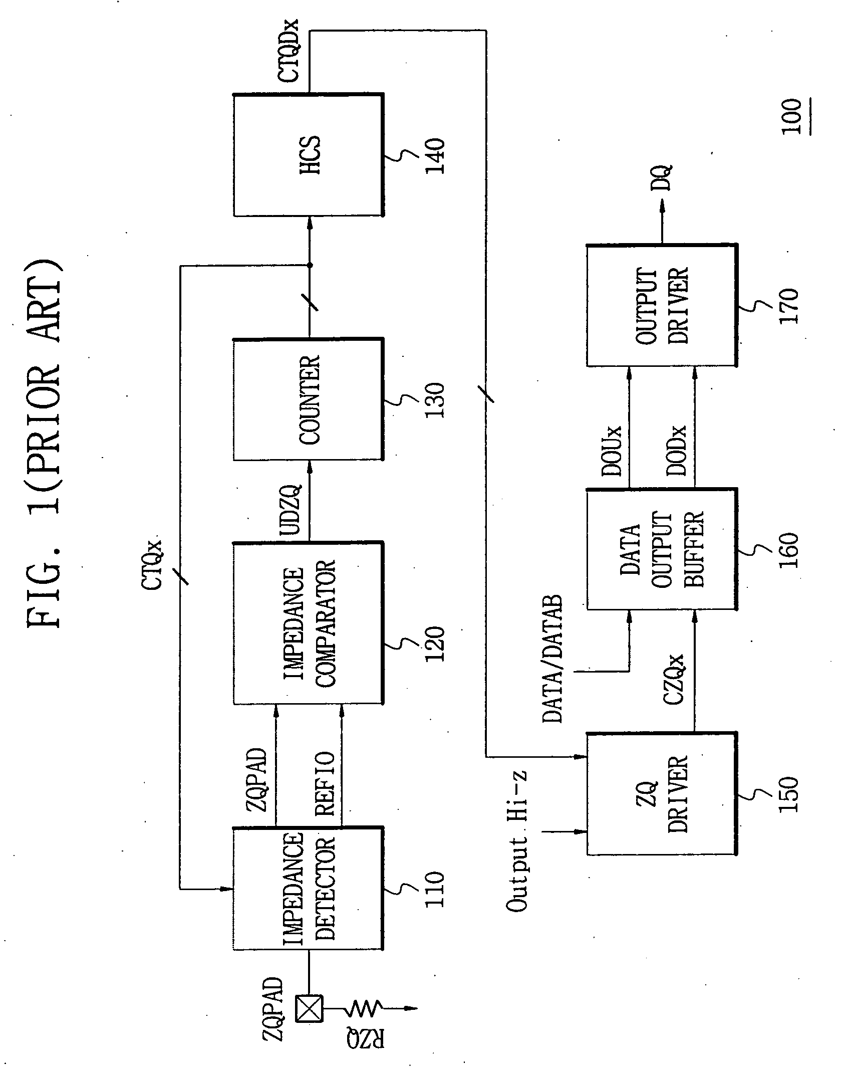
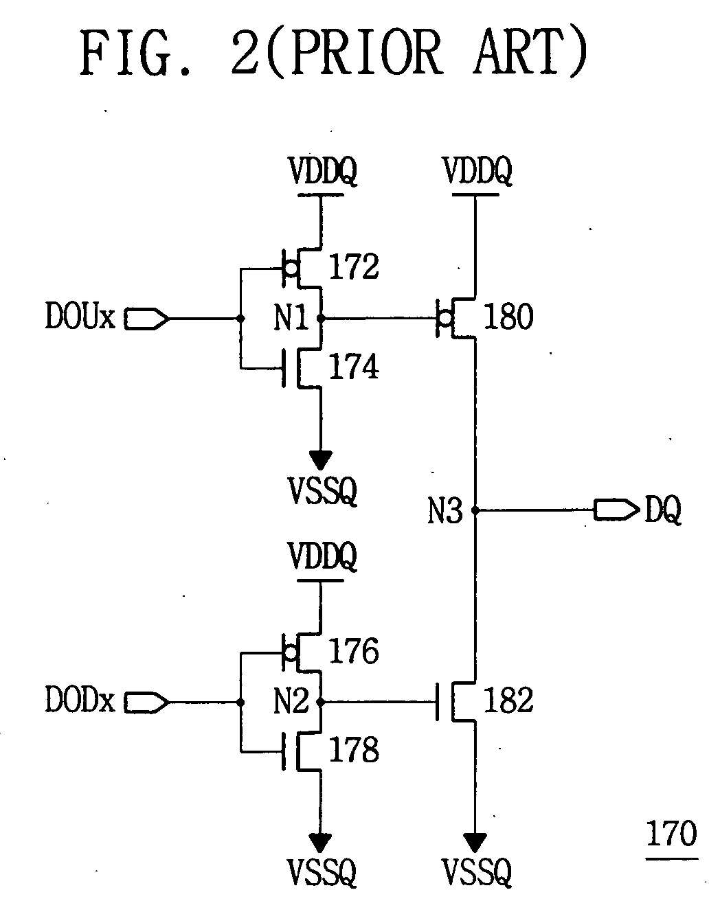
[0034]FIG. 3 is a circuit diagram showing a first driver for a data output circuit for use in a semiconductor device in accordance with an embodiment of the present invention, and FIG. 4 is a circuit diagram showing a second driver of a data output circuit for use in a semiconductor device in accordance with an embodiment of the present invention. Referring to FIG. 3, a first driver 200 for an output driver in accordance with an embodiment of the present invention includes a pull-up driver section for reducing an impedance change for applied pull-up output data DOUx in response to the pull-up output data and providing it to an output terminal DQ, and a pull-down driving section for reducing an impedance change for applied pull-down output data DODx in response to the pull-down output data and providing it to the output terminal DQ. The pull-up driving section includes a first PMOS transistor 202 connected between a first node N1 and an external power supply VDDQ and operating in res...


PUM


Abstract

There is provided an output driver for use in a semiconductor device capable of remarkably improving linearity of impedance by reducing or minimizing a change of an impedance for output data caused due to a change of an external power supply. The output driver for outputting internal data of a semiconductor device to the exterior of a chip comprises a first driving section including a driving transistor to maintain an impedance for applied data at a certain level in response to the data; and a second driving section for compensating for linearity of the impedance in response to an operation signal from the driving transistor of the first driving section and providing an output terminal with the data.

Description

CROSS-REFERENCE TO RELATED APPLICATION [0001] This application claims the benefit of Korean Patent Application No. 2004-2137, filed on Jan. 13, 2004, the contents of which are hereby incorporated herein by reference in their entirety. BACKGROUND [0002] 1. Technical Field [0003] The present invention relates to a semiconductor device and, more particularly, to an output driver for use in a semiconductor device capable of outputting internal data of the semiconductor device to the exterior of a chip. [0004] 2. Discussion of the Related Art [0005] Semiconductor devices, such as microcomputers, memory devices, gate arrays and the like, are used in a variety of electrical products such as personal computers, workstations and the like. Such semiconductor devices have input / output pins for transmitting and receiving data to and from external circuits, and an output circuit for providing internal data to external circuits, for example, an output buffer and an output driver circuit. When the...

Claims


Application Information

Patent Timeline
IPC IPC(8): G11C7/10H03K19/003
CPCH03K19/00384B65H54/71B65H73/00D01H11/00
Inventor CHOI, MYUNG-HANKIM, HWA-JINLEE, YOUNG-DAE
Owner SAMSUNG ELECTRONICS CO LTD
Why Eureka
Try Eureka