Thin film formation method, thin film formation equipment, method of manufacturing organic electroluminescence device, organic electroluminescence device, and electronic apparatus

a technology of thin film and vapor deposition, which is applied in the direction of individual semiconductor device testing, semiconductor/solid-state device testing/measurement, instruments, etc., can solve the problems of poor yield, high precision and exact vapor deposition cannot be carried out, etc., and achieve high precision and yield improvement

Inactive Publication Date: 2005-07-14
SEIKO EPSON CORP
View PDF12 Cites 79 Cited by
  • Summary
  • Abstract
  • Description
  • Claims
  • Application Information

AI Technical Summary

Benefits of technology

[0025] A method of manufacturing an organic EL device according to the present invention is the method of manufacturing an organic EL device that is formed by adhering each of a plurality of different materials to the substrate in a predetermined pattern, wherein the above described thin film formation method is used. Thin film made of each of a plurality of different materials can be formed in a predetermined pattern, on the substrate. Moreover, the predetermined pattern can be formed correctly with high precision. Accordingly, the occurrence of the defects such as that of the material mixing in with the other color pixels, which is the conventional problem, can be suppressed, and yield improvement can be attained.
[0026] An organic EL device according to the present invention is manufactured by using the above described manufacturing method. In this way, an organic EL device having pixels without color mixing and a clear picture display will be made.

Problems solved by technology

However, because the thermal expansion coefficient of the metal mask is very large as compared with the glass substrate for the panel, the metal mask expands larger than the glass substrate for the panel by radiation heat effect at the time of the vapor deposition as the panel size becomes large, which causes stress, and lifting due to this stress occurs in a portion which a magnet is attracting.
Thereby, there is a problem that a highly precise and exact vapor deposition cannot be carried out.
For example, defects such as that of material frequently mixing in with the other color pixels, and a problem of very poor yield occurs.

Method used


Image

  • Thin film formation method, thin film formation equipment, method of manufacturing organic electroluminescence device, organic electroluminescence device, and electronic apparatus
  • Thin film formation method, thin film formation equipment, method of manufacturing organic electroluminescence device, organic electroluminescence device, and electronic apparatus
  • Thin film formation method, thin film formation equipment, method of manufacturing organic electroluminescence device, organic electroluminescence device, and electronic apparatus

Examples


first embodiment

[0037] First Embodiment of the Mask Vapor Deposition Equipment

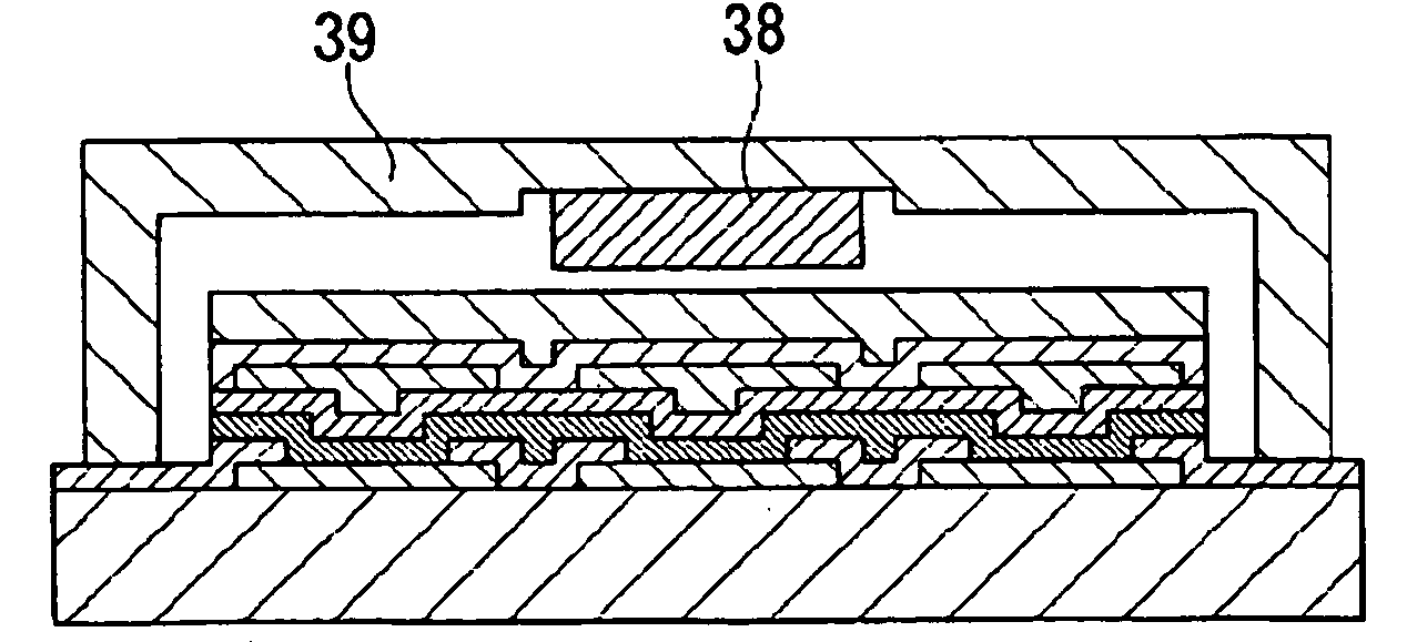
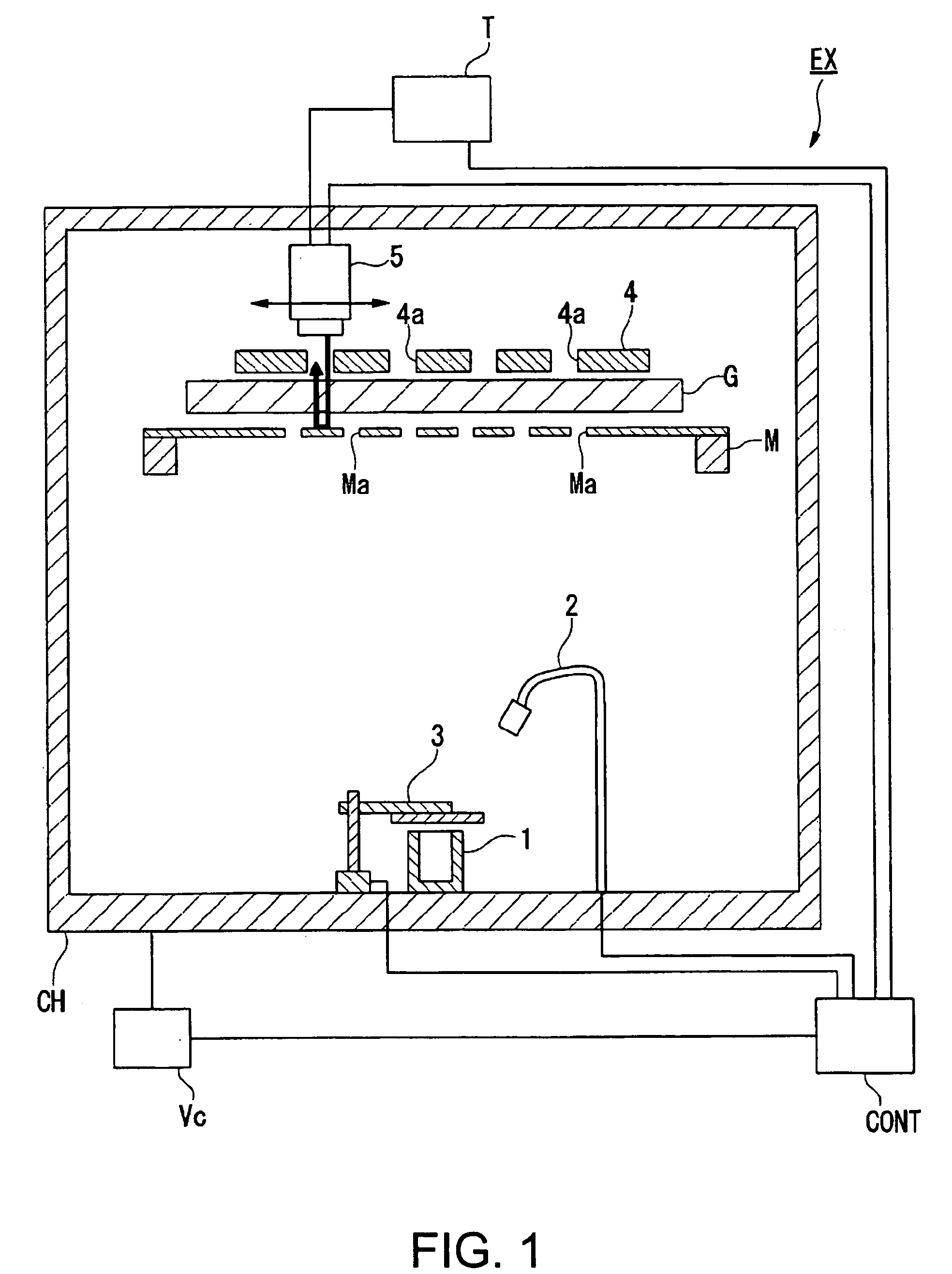
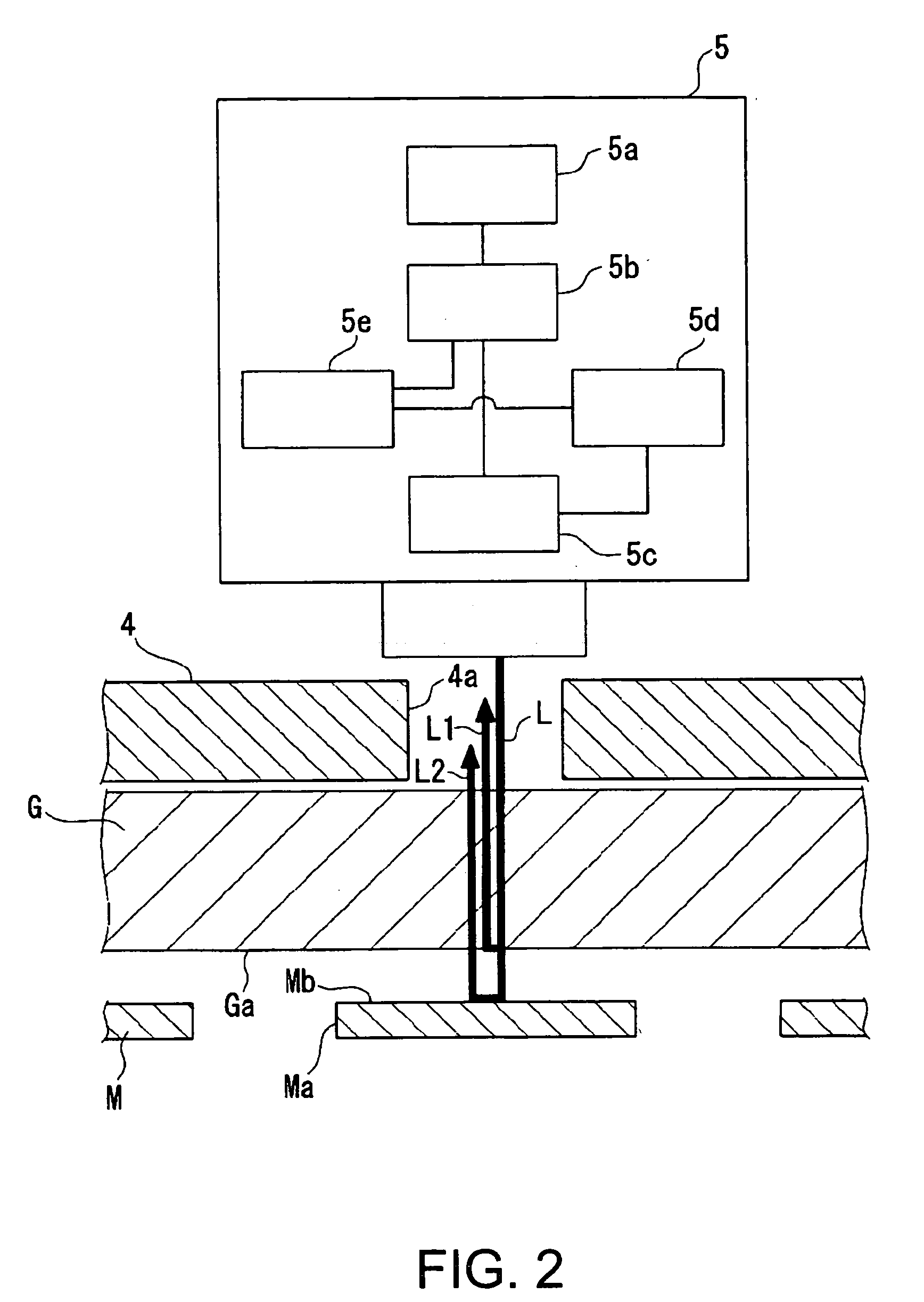
[0038]FIG. 1 is the cross-sectional side view showing the outline structure of the mask vapor deposition equipment (thin film formation equipment) of the present invention. As shown in FIG. 1, a mask vapor deposition equipment EX is provided with a vapor deposition source 1 (material source, thin film formation means), a film-thickness sensor 2, and a shutter (thin film formation means) 3 in the lower part of a chamber CH. Mask vapor deposition equipment EX is further provided with a vapor deposition mask M, a substrate G targeted for the vapor deposition, a sheet magnet (substrate contacting means) 4, and a laser displacement gauge (gap measurement means) 5 in the upper part of the chamber CH. Mask vapor deposition equipment EX is still further provided with an exhaust means Vc, a displacement device (displacement means) T, and a control device (control means) CONT on the outside of the chamber CH.

[0039] Next, each cons...

second embodiment

[0064] Second Embodiment of the Mask Vapor Deposition Equipment

[0065] Next, a second embodiment of the mask vapor deposition equipment will be described. In the first embodiment and its modification of the mask vapor deposition equipment described above, the sheet magnet 4 and the electromagnet are employed as the substrate contacting means. However, in this embodiment, the substrate and the mask are pressed and contacted by applying a load. In addition, in this embodiment, portions different from the mask vapor deposition equipment EX shown in FIG. 1 will be described. Moreover, the same numerals will be given to the same compositions as those of the above described embodiment to simplify the description.

[0066] As shown in FIG. 4, mask vapor deposition equipment EX′ is constituted comprising a load application portion 14 as the substrate contacting means, and a mask M′ made of non-magnetic material. The load application portion 14 consists of a weight 15, a pin 16, and an elastic ...


PUM

PropertyMeasurementUnit
work functionaaaaaaaaaa
sizeaaaaaaaaaa

Abstract

A thin film formation method is provided which can carry out various kinds of patterning deposition correctly and with high precision, and a thin film formation equipment. The thin film formation method arranges a mask between a substrate and a material source and forms the material of the material source as a thin film on the substrate. The method further includes: a substrate contacting process to contact the mask and the substrate; a gap measurement process to measure a gap between the mask and the substrate; and a thin film formation process to form the thin film according to the measurement result in the gap measurement process.

Description

RELATED APPLICATIONS [0001] This application claims priority to Japanese Patent Application Nos. 2003-431921 filed Dec. 26, 2003 and 2004-368619 filed Dec. 21, 2004 which are hereby expressly incorporated by reference herein in their entirety. BACKGROUND [0002] 1. Field of the Invention [0003] The present invention relates to a thin film formation method, thin film formation equipment, a method of manufacturing an organic electroluminescence device, an organic electroluminescence device, and an electronic apparatus. [0004] 2. Related Art [0005] Because an organic electroluminescence (hereinafter, referred to as organic EL) device is a self-luminescence type, high-speed response display element that has a structure of deposited thin films, a display panel which is light-weight and excellent in dealing with moving-pictures can be formed. Therefore, in recent years, much attention has been paid to the organic EL as a display panel, such as FPD (Flat Panel Display) television. As for th...

Claims


Application Information

Patent Timeline
Patent Type & Authority Applications(United States)
IPC IPC(8): H05B33/10C23C4/00C23C4/12C23C14/04C23C14/12C23C14/24H01L51/50
CPCC23C4/005C23C14/042C23C4/12C23C4/01H05B33/10
Inventor YOTSUYA, SHINICHI
Owner SEIKO EPSON CORP
Why Eureka
Try Eureka