Electronic component mounting method and apparatus
Inactive Publication Date: 2005-07-21
PANASONIC CORP
View PDF31 Cites 59 Cited by
Summary
Abstract
Description
Claims
Application Information
AI Technical Summary
This helps you quickly interpret patents by identifying the three key elements:
Problems solved by technology
Method used
Benefits of technology
Benefits of technology
[0020] a tip of the formed bump is shaped so as to prevent collapse of a neck portion of the bump by once pressurizing the bump with a load of not greater than 20 gf.
[0108] According to a 39th aspect of the present invention, there is provided an electronic component mounting method as defined in the 37th or 38th aspect, wherein the portion brought in contact with the electronic component is provided by an insulating resin that improves adhesion to a film material used on a surface of the electronic component, and the portion brought in contact with the board is provided by an insulating resin that improves adhesion to a material used on a surface of the board.
Problems solved by technology
According to the above-mentioned method called SMT (Surface Mount Technology), the process of packaging the IC is long and requires much time for the production of IC components, and it has been difficult to miniaturize the circuit board.
However, any of the processing methods has had the drawback that much time is required for the hardening of the paste for bonding the bumps of the IC chip to the electrodes of the board and for the coating and hardening of the encapsulation resin, leading to degraded productivity.
There has also been the issue that ceramic or glass of which the quantity of warp is controlled is needed as a circuit board, leading to cost increase.
However, it is difficult to uniformly disperse the conductive particles in the conductive adhesive, and this has disadvantageously caused short circuit due to the abnormal dispersion of the particles and led to the expensive cost of the conductive adhesive and the necessity of the formation of the IC chip bumps by electroplating in order to shape the height of the bumps.
Moreover, according to the method of performing bonding using a UV-curing resin as in the third prior art, it is required to set a bump height variation within a range of ±1 (μm), and there has been the issue that the bonding cannot be achieved in the case of a board of a degraded flatness such as a resin board (glass epoxy board).
A time of two to eight hours has been needed for the hardening of the encapsulation resin, and this has led to the issue that the productivity is extremely degraded.
Method used
Image
Click on the blue label to locate the original text in one second.
Reading with bidirectional positioning of images and text.
Examples
tenth embodiment
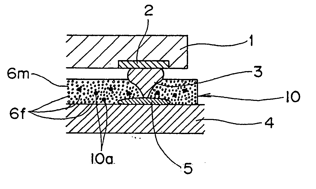
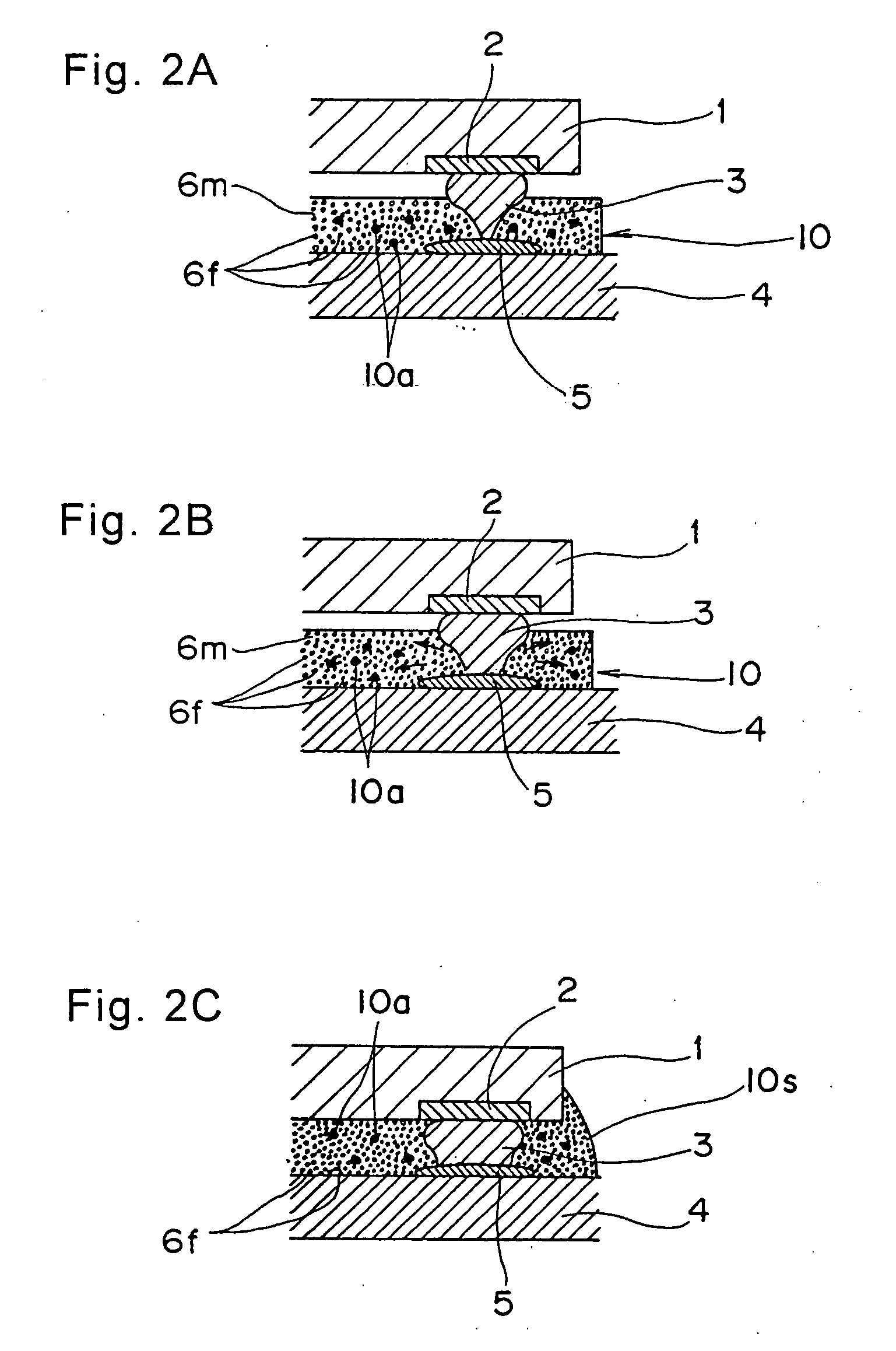
[0238] Next, according to a method and apparatus for mounting an electronic component, for example, an IC chip onto a circuit board, and an electronic component unit or module, for example, a semiconductor device in which the IC chip is mounted on the board by the mounting method, according to a tenth embodiment of the present invention will be described. In order to further ensure an effect of the ninth embodiment, a mean particle diameter of one inorganic filler 6f-1, of the inorganic fillers 6f-1 and 6f-2, is two or more times different from a mean particle diameter of the other inorganic filler 6f-2. As a concrete example, an inorganic filler having a mean particle diameter of 0.5 μm and an inorganic filler having a mean particle diameter of 2 to 4 μm are employed.
[0239] With this arrangement, the effect of the ninth embodiment can further be improved. That is, by mixing insulating resin 6m with inorganic fillers 6f-1 and 6f-2, which have the plurality of different mean particl...
eleventh embodiment
[0240] Next, according to a method and apparatus for mounting an electronic component, for example, an IC chip onto a circuit board, and an electronic component unit or module, for example, a semiconductor device in which the IC chip is mounted on the board by the mounting method, according to an eleventh embodiment of the present invention will be described. In order to further ensure an effect of the ninth embodiment, it is preferable to have the inorganic filler 6f, to be mixed with the insulating resin 6m, include at least two types of inorganic fillers 6f-1 and 6f-2, which have a plurality of different mean particle diameters, with one inorganic filler 6f-1 having a mean particle diameter exceeding 3 μm and the other inorganic filler 6f-2 having a mean particle diameter of not greater than 3 μm. As a concrete example, an inorganic filler having a mean particle diameter of 0.5 μm and an inorganic filler having a mean particle diameter of 2 to 4 μm are employed.
twelfth embodiment
[0241] Next, according to a method and apparatus for mounting an electronic component, for example, an IC chip onto a circuit board, and an electronic component unit or module, for example, a semiconductor device in which the IC chip is mounted on the board by the mounting method, according to a twelfth embodiment of the present invention will be described. Based on each of the aforementioned embodiments, it is acceptable to have the inorganic filler 6f, to be mixed with the insulating resin 6m, include at least two types of inorganic fillers 6f-1 and 6f-2, which have different mean particle diameters, and constitute inorganic filler 6f-1; having the larger mean particle diameter, from a material identical to that of the insulating resin 6m, thereby producing a stress alleviating effect. As a concrete example, an inorganic filler having a mean particle diameter of 0.5 μm and an inorganic filler having a mean particle diameter of 2 to 4 μm are employed.
[0242] According to this twelf...
PUM
Property
Measurement
Unit
Percent by mass
aaaaa
aaaaa
Angle
aaaaa
aaaaa
Weight
aaaaa
aaaaa
Abstract
A chip is bonded on a circuit board by aligning in position bumps with board electrodes with interposition of an anisotropic conductive layer between the chip and the circuit board. The anisotropic conductive layer is a mixture of an insulating resin, conductive particles and an inorganic filler. The chip is pressed against the board with a pressure force of not smaller than 20 gf per bump by virtue of a tool, while warp of the chip and the board is connected, the bumps are compressed, and the insulating resin is hardened.
Description
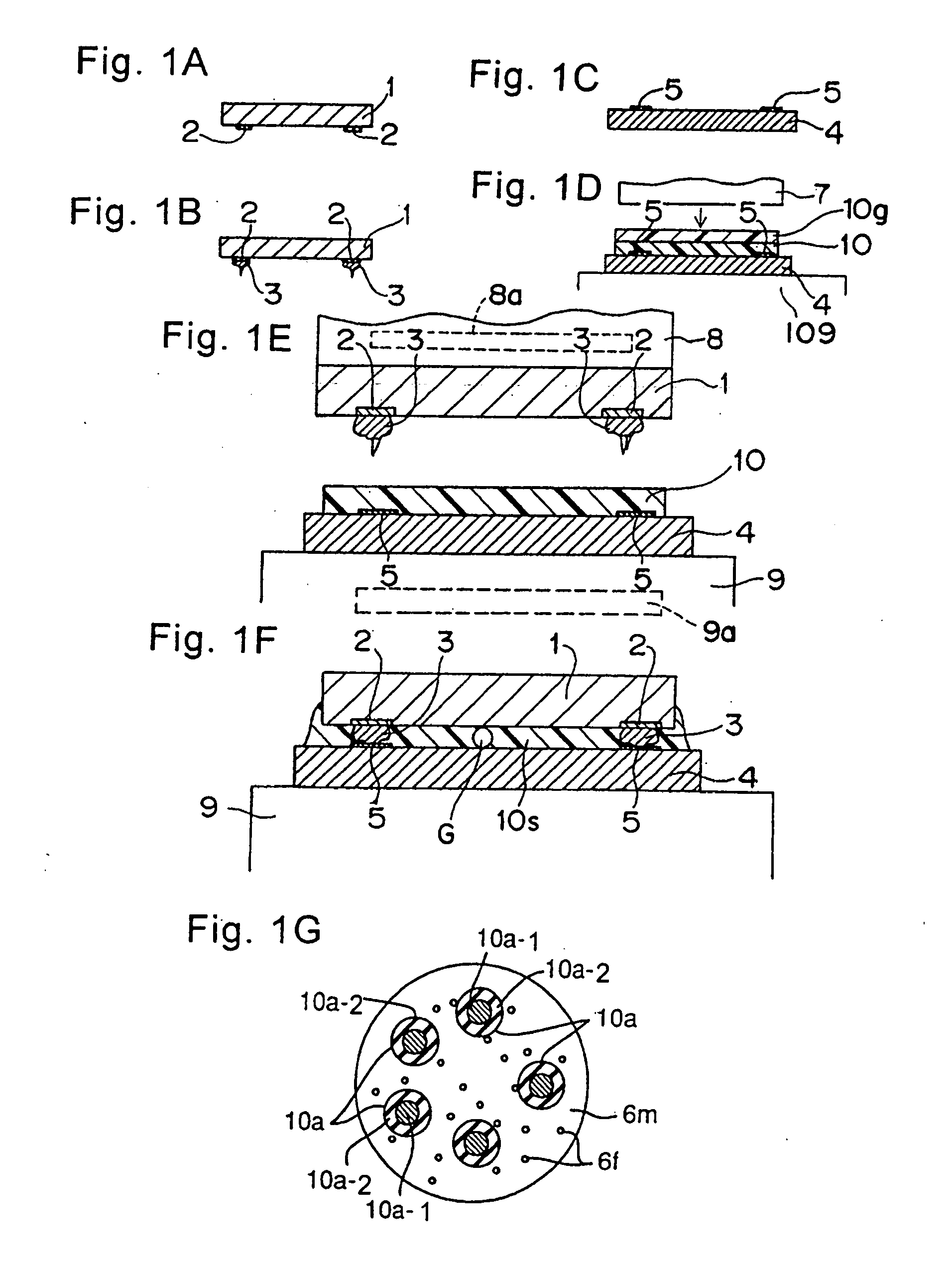
[0001] This application is a divisional of U.S. Ser. No. 09 / 890,066, filed Jul. 26, 2001, which is a National Stage of International Application No. PCT / JP00 / 00372, filed Jan. 26, 2000.TECHNICAL FIELD [0002] The present invention relates to an electronic component method and apparatus for mounting on a circuit board an electronic component of, for example, an IC chip and a surface acoustic wave (SAW) device on an electronic circuit use printed board (referred to as a “board” as a representative example in the present specification, and the “board” means a mounting base object on which other components such as an interposer and / or an electronic component are mounted) in a single body (a bear IC in the case of an IC chip) state, and relates to an electronic component unit obtained by mounting the electronic components on the board by the mounting method. BACKGROUND ART [0003] In these days, electronic circuit boards have come to be used in various sorts of products, and the performanc...
Claims
Application Information
Patent Timeline
Application Date:The date an application was filed.
Publication Date:The date a patent or application was officially published.
First Publication Date:The earliest publication date of a patent with the same application number.
Issue Date:Publication date of the patent grant document.
PCT Entry Date:The Entry date of PCT National Phase.
Estimated Expiry Date:The statutory expiry date of a patent right according to the Patent Law, and it is the longest term of protection that the patent right can achieve without the termination of the patent right due to other reasons(Term extension factor has been taken into account ).
Invalid Date:Actual expiry date is based on effective date or publication date of legal transaction data of invalid patent.

