Hierarchical assembly of interconnects for molecular electronics

a technology of molecular electronics and interconnections, applied in the field of nanotechnology devices and fabrication methods therefor, can solve problems such as contact and charge transport in nanoscale electronic molecules, and achieve the effect of facilitating spectroscopic characterization

Inactive Publication Date: 2005-07-21
NORTH CAROLINA STATE UNIV
View PDF3 Cites 23 Cited by
  • Summary
  • Abstract
  • Description
  • Claims
  • Application Information

AI Technical Summary

Benefits of technology

[0006] It is known that transistor behavior can be exhibited in single molecules.3,4 These results illustrated the concept of gain, and correlated current-voltage behavior with other properties of the molecule (e.g., a change in spin state). However, embodiments of the present invention can provide gain as the result of a state change within the molecular architecture rather than as the response of a molecule to a change in bias of an underlying (macroscopic) gate electrode. Moreover, an open architecture of some embodiments of the invention can facilitate spectroscopic characterization in addition to correlation of current-voltage behaviors with molecular properties. Finally, embodiments of the invention can bridge the lithographic and molecular length scales by room temperature, orthogonal self-assembly. This strategy can offer the possibility of larger scale integration, rather than making devices in a sequential (one at a time) fashion.

Problems solved by technology

While silicon technology continues to extend into regimes that may have been previously thought to be difficult or even impossible, the field of molecular-based electronic materials and devices is beginning to gain interest as a potential future challenge or extension to silicon.
For example, there may be challenges in contact and charge transport in nanoscale electronic molecules.

Method used


Image

  • Hierarchical assembly of interconnects for molecular electronics
  • Hierarchical assembly of interconnects for molecular electronics
  • Hierarchical assembly of interconnects for molecular electronics

Examples


Embodiment Construction

[0024] The present invention now will be described more fully hereinafter with reference to the accompanying drawings, in which embodiments of the invention are shown. This invention may, however, be embodied in many different forms and should not be construed as limited to the embodiments set forth herein. Rather, these embodiments are provided so that this disclosure will be thorough and complete, and will fully convey the scope of the invention to those skilled in the art. In the drawings, the sizes and relative sizes of layers and regions may be exaggerated for clarity.

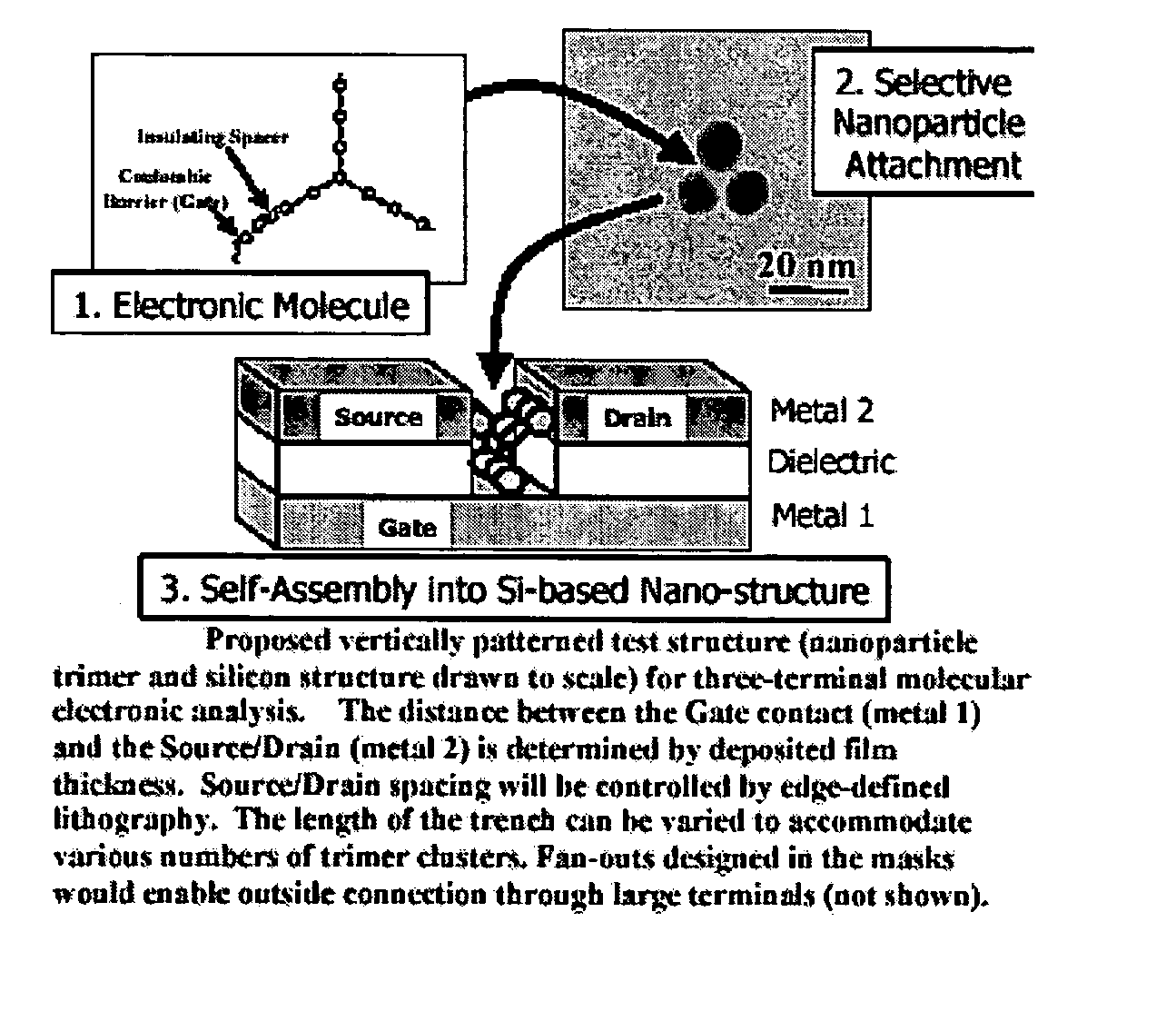
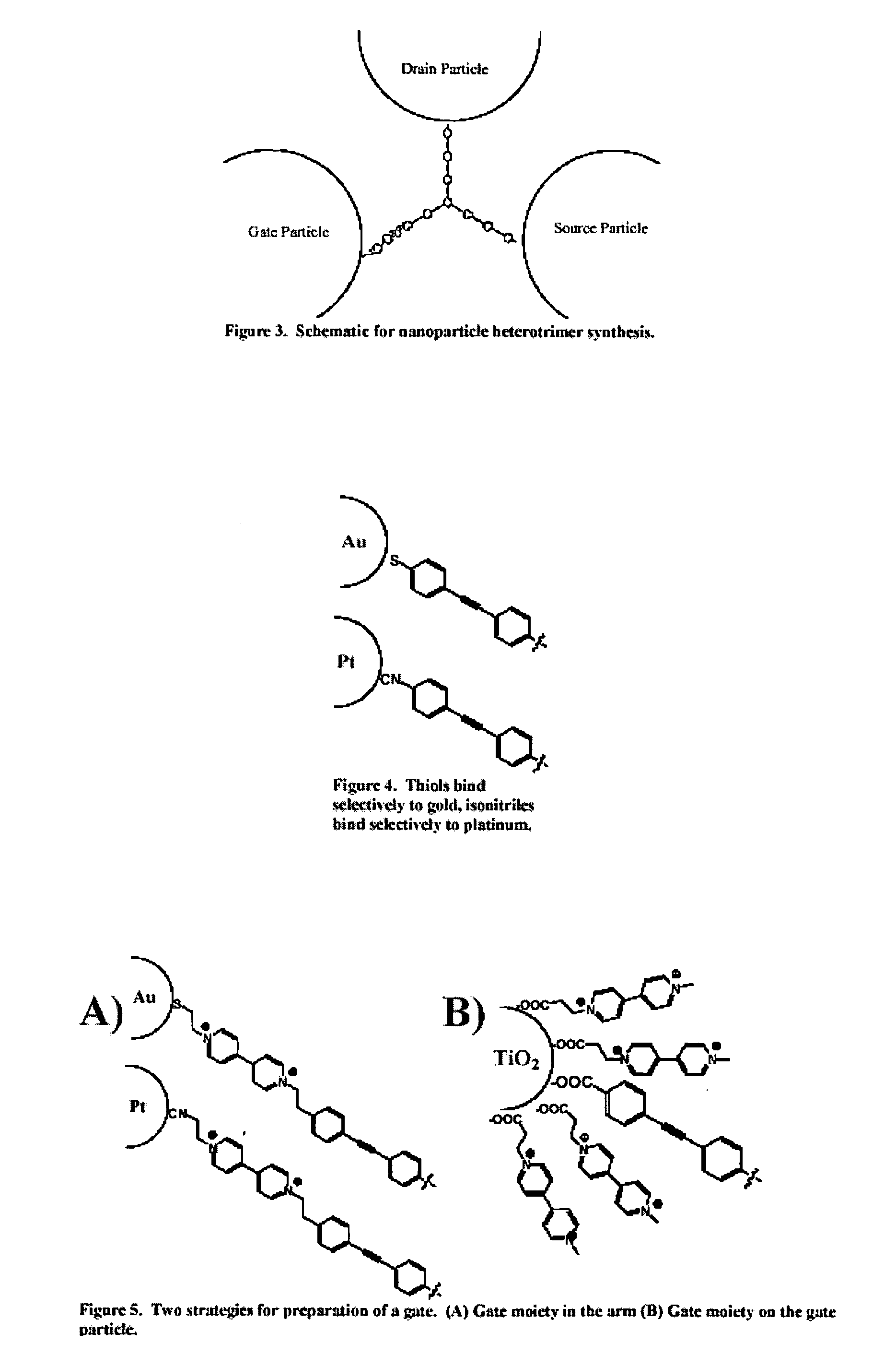
[0025] Some embodiments of the invention can provide self-assembly methods that can bridge two- and / or three-terminal molecules to electrodes. Gain may be demonstrated at the molecular level using a three-terminal molecular wiring scheme. Gain has been demonstrated using gate electrodes placed under or beside collections of two-armed molecules. Although the electronic properties of such architectures can provide ...


PUM


Abstract

A hierarchical assembly methodology can interconnect individual two- and / or three-terminal molecules with other nanoelements (nanoparticles, nanowires, etc.) to form solution-based suspensions of nanoscale assemblies. The nanoassemblies can then undergo chemical-selective alignment and attachment to nanopatterned silicon and / or other surfaces for interconnection and / or measurement.

Description

CROSS-REFERENCE TO RELATED APPLICATION [0001] This application claims the benefit of provisional Application No. 60 / 489,009, filed Jul. 21, 2003, entitled Hierarchical Assembly of Interconnects for Molecular Electronics, the disclosure of which is hereby incorporated herein by reference in its entirety as if set forth fully herein.FIELD OF THE INVENTION [0002] This invention relates to microelectronic devices and fabrication methods therefor, and more particular to nanotechnology devices and fabrication methods therefor. BACKGROUND OF THE INVENTION [0003] While silicon technology continues to extend into regimes that may have been previously thought to be difficult or even impossible, the field of molecular-based electronic materials and devices is beginning to gain interest as a potential future challenge or extension to silicon. Recent news that molecular systems can be used to achieve current gain1,2 may heighten interest. Demonstration of gain in a molecular electronic system ma...

Claims


Application Information

Patent Timeline
Patent Type & Authority Applications(United States)
IPC IPC(8): H01L23/532H01L51/00H01L51/05H01L51/30H01L51/40
CPCB82Y10/00G11C13/02H01L23/53276H01L51/0021H01L51/0051H01L51/0062H01L2924/0002H01L51/0077H01L51/0545H01L51/0595H01L2924/00H10K71/60H10K85/611H10K85/649H10K85/30H10K10/466H10K10/701
Inventor PARSONS, GREGORY N.FELDHEIM, DANIEL L.GORMAN, CHRISTOPHER B.
Owner NORTH CAROLINA STATE UNIV
Why Eureka
Try Eureka