Refractory metal nitride barrier layer with gradient nitrogen concentration

a technology of refractory metal nitride and barrier layer, which is applied in the direction of semiconductor devices, semiconductor/solid-state device details, electrical apparatus, etc., can solve the problems that the use of such barrier materials often compromises the electrical performance of microelectronic fabrication, and achieves the effect of being ready to manufactur

Inactive Publication Date: 2005-07-21
TAIWAN SEMICON MFG CO LTD
View PDF6 Cites 12 Cited by
  • Summary
  • Abstract
  • Description
  • Claims
  • Application Information

AI Technical Summary

Benefits of technology

[0015] A second object of the present invention is to provide the conductor structure and the method for fabricating the conductor structure in accord with the first object of the present invention, wherein the conductor structure has inhibited interdiffusion and enhanced performance such as improved electromigration resistance.
[0016] A third object of the present invention is to provide a conductor structure and a method for fabricating the conductor structure in accord with the first object of the present invention and the second object of the present invention, wherein the conductor structure is readily fabricated.
[0019] Within the present invention, when a barrier layer in accord with the present invention is employed as a barrier layer with respect to a copper containing conductor layer within a microelectronic conductor structure, the microelectronic conductor structure is formed with inhibited interdiffusion and enhanced performance.
[0020] The present invention provides a barrier layer for use within a microelectronic conductor structure for use within a microelectronic fabrication, wherein the microelectronic fabrication is fabricated with inhibited interdiffusion and enhanced performance.
[0022] A microelectronic conductor structure within a microelectronic fabrication having formed therein a barrier layer in accord with the present invention is readily fabricated.

Problems solved by technology

While copper containing conductor materials are thus desirable in the art of microelectronic fabrication for forming patterned microelectronic conductor layers within microelectronic fabrications, copper containing conductor materials are nonetheless not entirely without problems in the art of microelectronic fabrication for forming patterned microelectronic conductor layers within microelectronic fabrications.
In that regard, patterned microelectronic conductor materials formed of copper containing conductor materials within microelectronic fabrications are often susceptible to interdiffusion with adjoining microelectronic materials formed within microelectronic fabrications.
Similarly, while barrier layers and barrier materials are known in the art of microelectronic fabrication for inhibiting interdiffusion of copper containing conductor materials within microelectronic fabrications, use of such barrier materials often compromises electrical performance of microelectronic fabrications.

Method used


Image

  • Refractory metal nitride barrier layer with gradient nitrogen concentration
  • Refractory metal nitride barrier layer with gradient nitrogen concentration
  • Refractory metal nitride barrier layer with gradient nitrogen concentration

Examples


examples

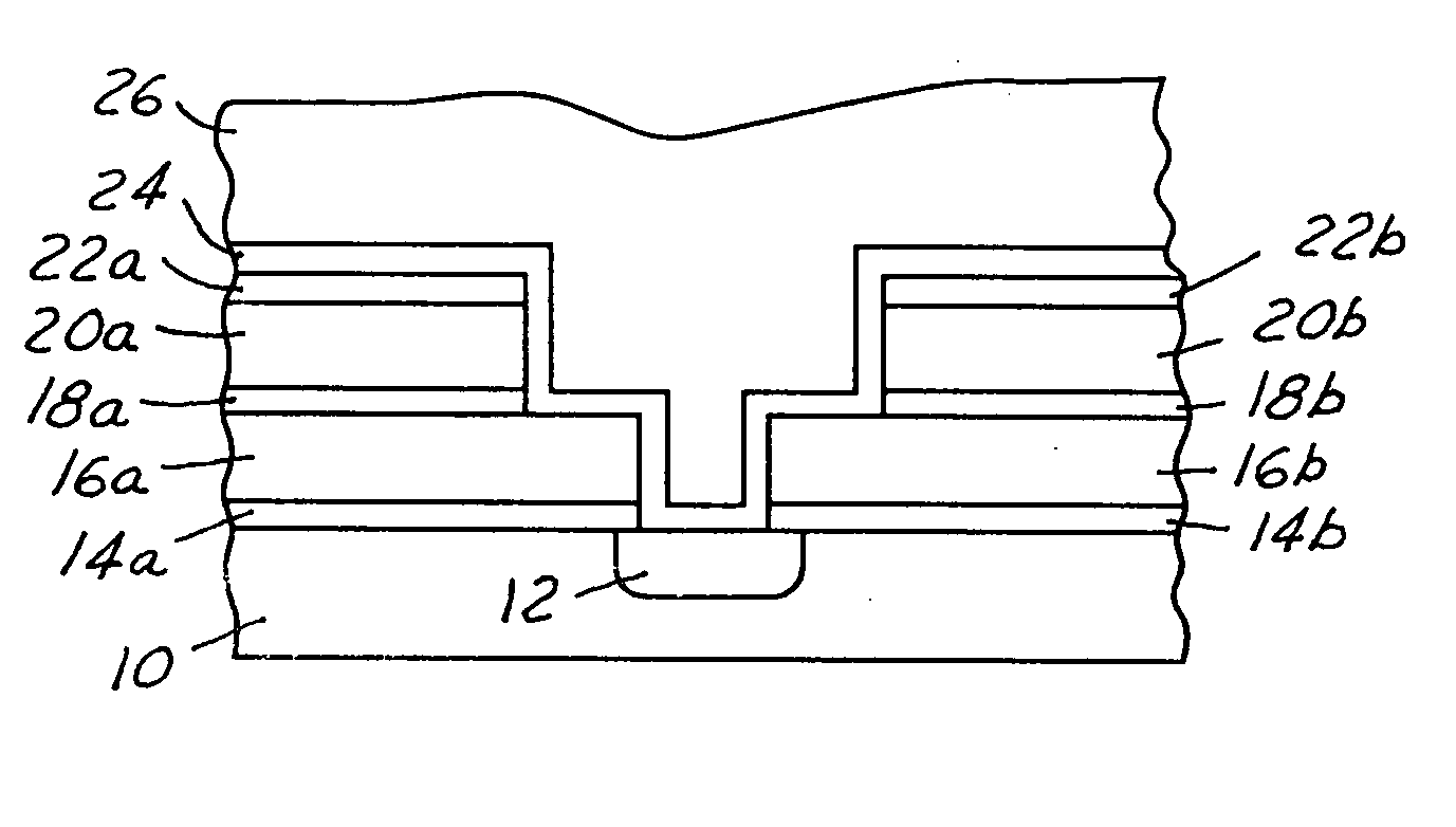
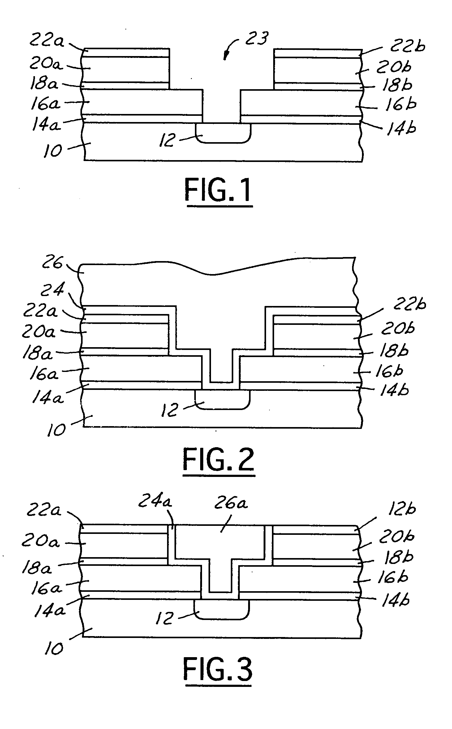
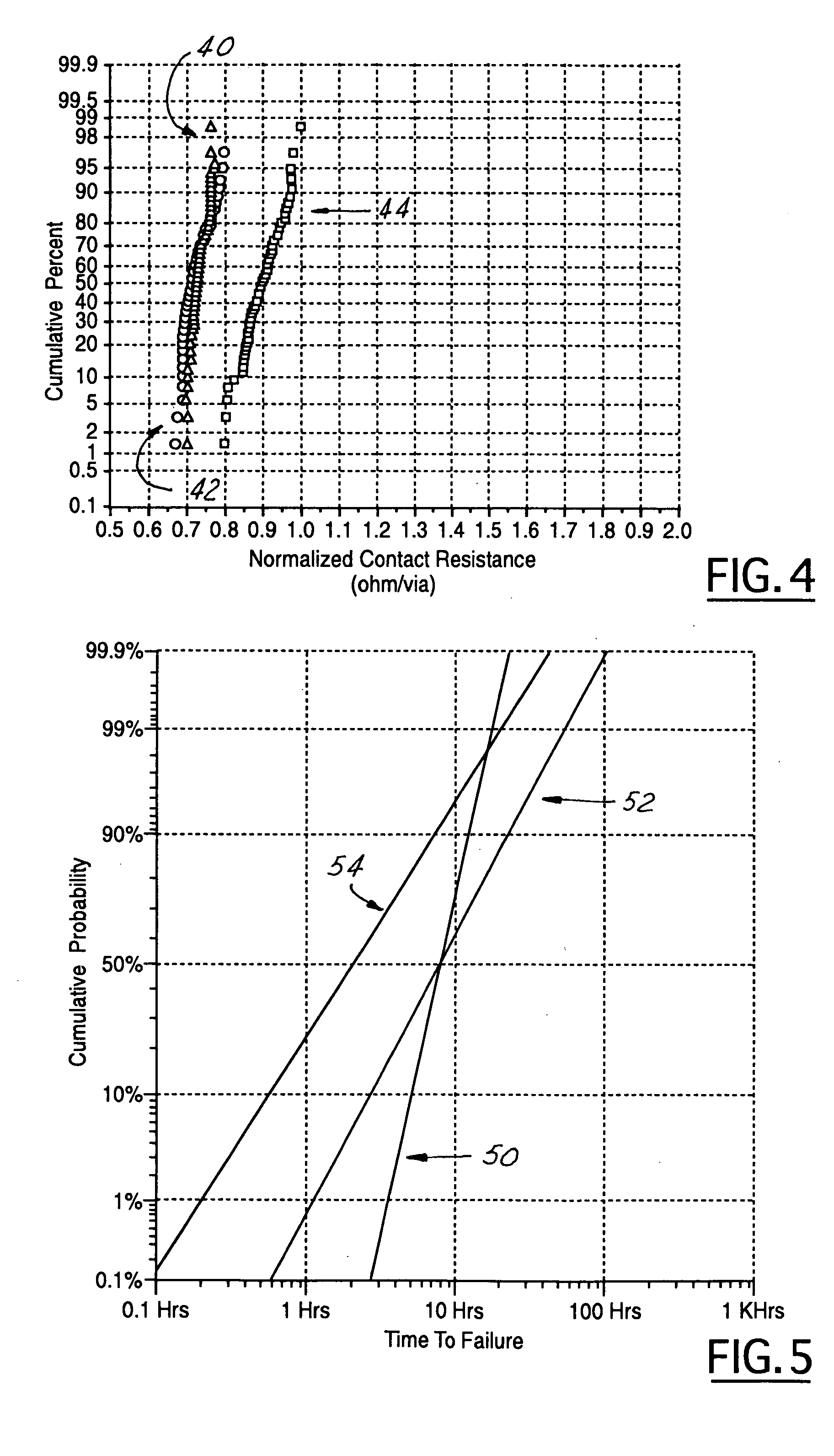
[0057] In order to illustrate the value of the present invention, there was fabricated three series of microelectronic fabrications generally in accord with the microelectronic fabrication whose schematic cross-sectional diagram is illustrated in FIG. 3, but wherein there was formed within each of the three series of microelectronic fabrications a patterned conductor barrier layer formed of one of three different compositions. A first of the three different compositions was a tantalum nitride barrier layer formed in accord with the present invention, wherein the tantalum nitride barrier layer was formed of a substantially stoichiometric tantalum nitride material layer of thickness about 90 angstroms, having formed thereupon a nitrogen deficient tantalum nitride material layer of tantalum:nitrogen atomic ratio about 1:0.3 of thickness about 130 angstroms, in turn having formed thereupon a tantalum material layer formed to a thickness of about 30 angstroms. A second of the three diffe...


PUM

PropertyMeasurementUnit
thicknessaaaaaaaaaa
thicknessaaaaaaaaaa
thicknessaaaaaaaaaa

Abstract

Within a microelectronic fabrication and a method for fabricating the microelectronic fabrication a barrier layer is formed over a substrate. Within the method and the microelectronic fabrication the barrier layer is formed of a refractory metal nitride barrier material having within its thickness a gradient in nitrogen concentration. The barrier layer has low resistivity and improved electromigration performance.

Description

BACKGROUND OF THE INVENTION [0001] 1. Field of the Invention [0002] The present invention relates generally to refractory metal nitride layers within microelectronic fabrications. More particularly, the present invention relates to refractory metal nitride layers with enhanced performance within microelectronic fabrications. [0003] 2. Description of the Related Art [0004] Microelectronic fabrications are formed from microelectronic substrates over which are formed patterned microelectronic conductor layers which are separated by microelectronic dielectric layers. [0005] As microelectronic fabrication integration levels have increased and patterned microelectronic conductor layer dimensions have decreased, it has become increasingly common in the art of microelectronic fabrication to fabricate within microelectronic fabrications patterned microelectronic conductor layers formed of copper containing conductor materials. Patterned microelectronic conductor layers formed within microele...

Claims


Application Information

Patent Timeline
Patent Type & Authority Applications(United States)
IPC IPC(8): H01L21/285H01L21/768
CPCH01L21/76846H01L21/2855
Inventor LEE, HSIEN-MINGPAN, SHING-CHYANGLIU, CHUNG-SHIYU, CHEN-HUA
Owner TAIWAN SEMICON MFG CO LTD
Why Eureka
Try Eureka