Image display device

a display device and image technology, applied in static indicating devices, instruments, electroluminescent light sources, etc., can solve the problems of increased electrical power consumption, complicated production processes, and increased production complexity

Active Publication Date: 2005-07-21
INNOLUX CORP
View PDF8 Cites 20 Cited by
  • Summary
  • Abstract
  • Description
  • Claims
  • Application Information

AI Technical Summary

Benefits of technology

[0011] It is an object of the present invention to at least solve the problems in the conventional technology.
[0012] A image display device according to one aspect of the present invention includes a light emitting unit that emits light by current injection; and a driving unit that includes a first terminal and a second terminal, and controls current flowing through the light emitting unit based on a potential difference applied between the first terminal and the second terminal. The potential difference is higher than a predetermined drive threshold. The image display device also includes a threshold potential detecting unit that detects the potential difference; a luminance potential supplying unit that changes the potential difference to a value lower than the drive threshold by a luminance potential corresponding to a luminance of the light emitting unit; and a sweep potential supplying unit that controls the driving unit by supplying a sweep potential to the first terminal after the potential changed by the luminance potential supplying unit. The sweep potential is swept in a range between a value lower than the luminance potential and a value higher than the luminance potential.

Problems solved by technology

However, because the conventional image display device using the OLED has a configuration in which the inverter 102 is included, there are problems in that production becomes complicated and electrical power consumption is increased.
When the thin film transistors having the different conduction types are formed on the same substrate, because it is necessary to produce the thin film transistors through the different processes, there are problems in that production processes becomes complicated and production cost is increased.

Method used


Image

  • Image display device
  • Image display device
  • Image display device

Examples


first embodiment

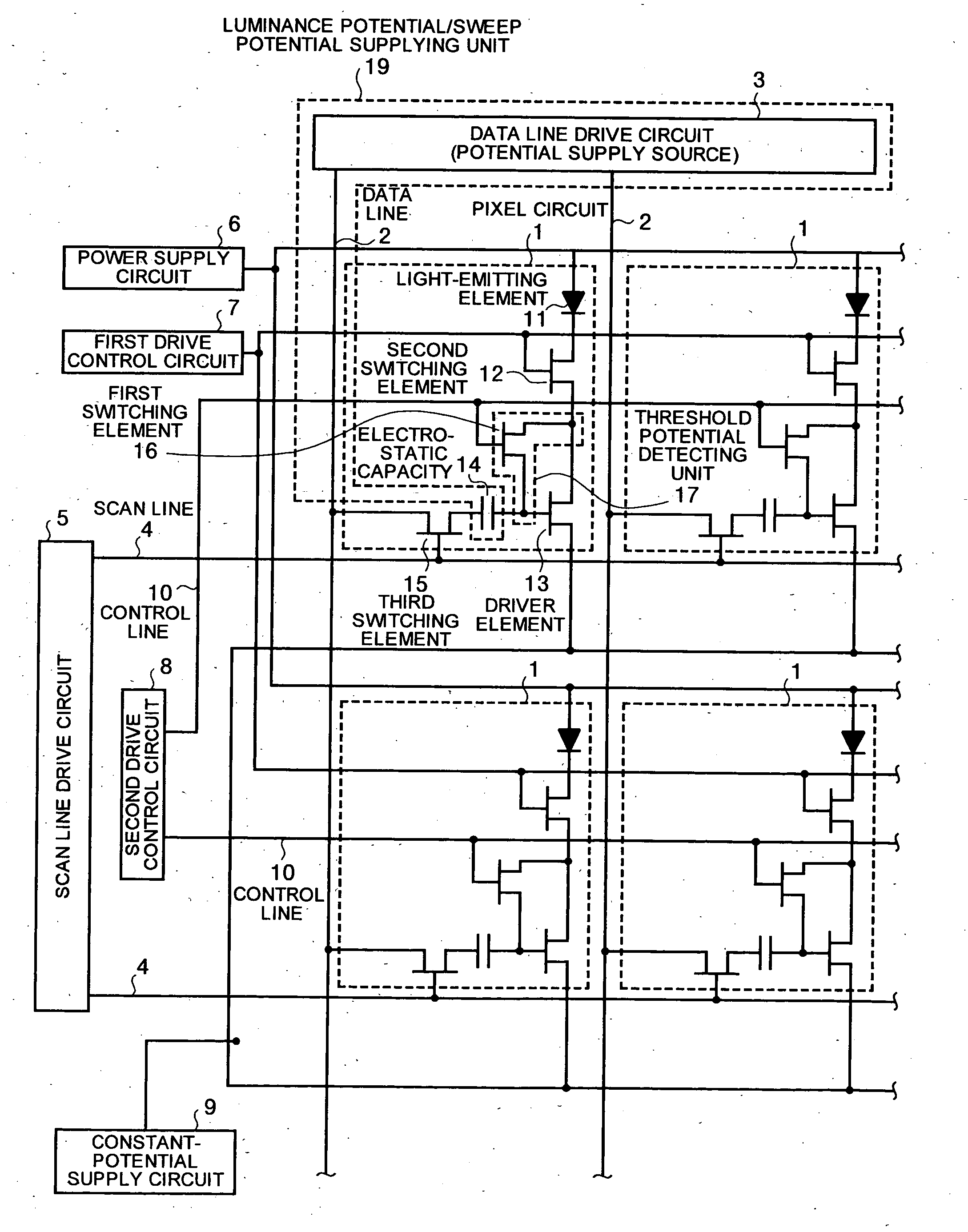
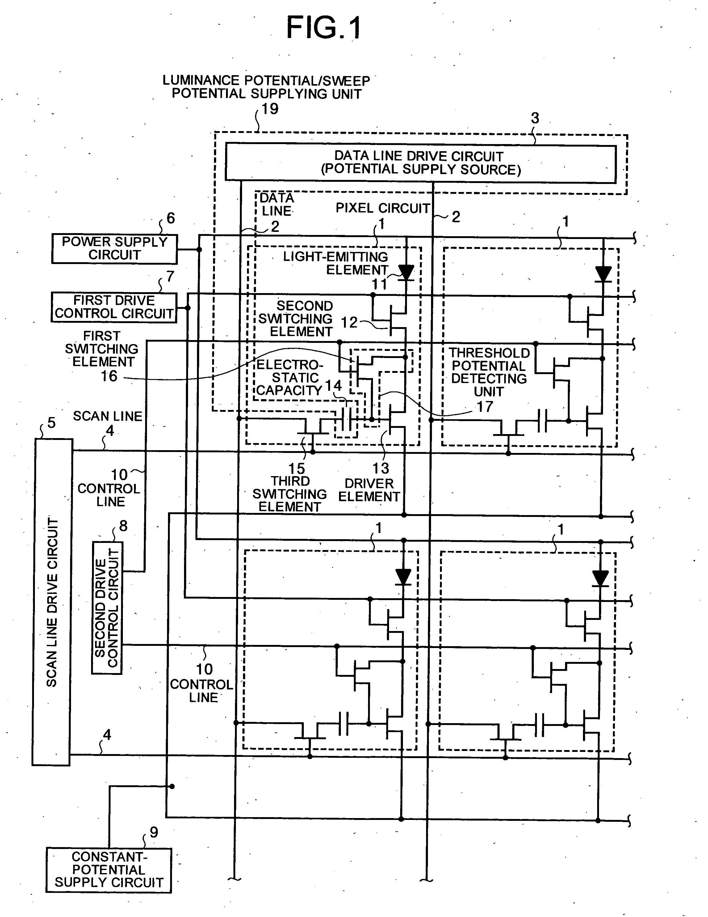
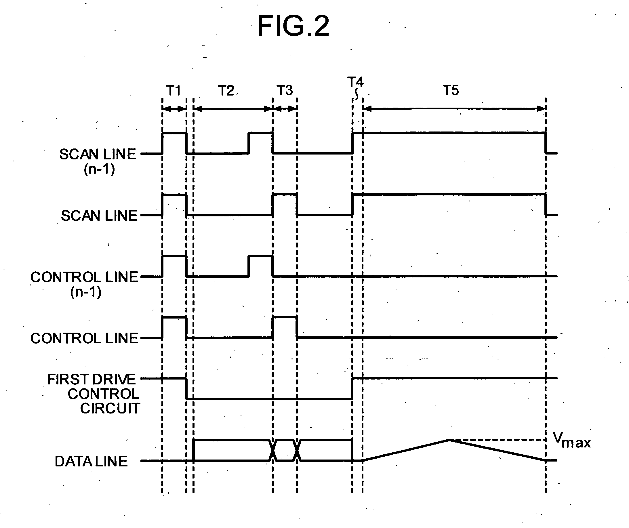
[0027] The second switching element 12 has the function of controlling the conduction between the light-emitting element 11 and the driver element 13. In the first embodiment, the second switching element 12 is formed by the n-type thin film transistor. That is, the second switching element 12 has the configuration in which the gate electrode of the thin film transistor is electrically connected to the first drive control circuit 7 while the drain electrode and the source electrode are connected to the light-emitting element 11 and the driver element 13 respectively, which controls the conduction state between the light-emitting element 11 and the driver element 13 based on the potential supplied from the first drive control circuit 7.

[0028] The driver element 13 has the function of controlling the time in which current passes through the light-emitting element 11. Specifically, the driver element 13 has the function of controlling the current passing through the light-emitting elem...

second embodiment

[0053]FIG. 5 is a block diagram of the image display device according to the As shown in FIG. 5, the image display apparatus includes a plurality of pixel circuits 31 arranged in the matrix shape, a data line drive circuit 33 that supplies the luminance potential to the pixel circuits 31 through a data line 32, and a scan line drive circuit 35 that supplies the scanning signal through a scan line 34, a power supply circuit 36 that supplies the drive power to the light-emitting element, a first drive control circuit 37 that supplies the potential for controlling the conduction state between the light-emitting element and the power supply circuit 36, a second drive control circuit 38 that supplies the potential in detecting the threshold voltage and the like, and a constant-potential supply circuit 39 that supplies the reference potential.

[0054] The pixel circuit 31 includes a light-emitting element 41 whose cathode side is electrically connected to the constant-potential supply circ...


PUM


Abstract

A image display device includes a driving unit that includes a first terminal and a second terminal, and controls current flowing through a light emitting unit based on a potential difference applied between the first terminal and the second terminal. The potential difference is higher than a predetermined drive threshold. The image display device also includes a threshold potential detecting unit that detects the potential difference; a luminance potential supplying unit that changes the potential difference to a value lower than the drive threshold by a luminance potential corresponding to a luminance of the light emitting unit; and a sweep potential supplying unit that controls the driving unit by supplying a sweep potential to the first terminal. The sweep potential is swept in a range between a value lower than the luminance potential and a value higher than the luminance potential.

Description

BACKGROUND OF THE INVENTION [0001] 1) Field of the Invention [0002] The present invention relates to an image display device that displays an image by changing a light-emission time according to display luminance. [0003] 2) Description of the Related Art [0004] In a drive circuit of the image display device using an organic light emitting diode (OLED), the drive circuit in which light-emission luminance of the OLED is not changed but a light-emission time of the OLED is changed has been proposed in order to realize display luminance in each pixel. That is, in any pixel, the light-emission time of the OLED is lengthened when high intensity display is performed, and the light-emission time is shortened when low intensity display is performed. [0005] As shown in FIG. 9A, the conventional image display device includes an OLED 101, an inverter 102 whose output terminal is connected to an anode side of the OLED, a thin film transistor 103 that functions as a switching element for resettin...

Claims


Application Information

Patent Timeline
Patent Type & Authority Applications(United States)
IPC IPC(8): H01L51/50G09G3/20G09G3/30G09G3/32H05B33/14
CPCG09G3/2014G09G3/3258G09G2300/0819G09G2320/043G09G2300/0861G09G2310/066G09G2300/0842
Inventor ONO, SHINYA
Owner INNOLUX CORP
Why Eureka
Try Eureka