Optical displacement sensor and optical encoder

a technology of optical encoder and optical displacement sensor, which is applied in the direction of converting sensor output optically, instruments, measurement devices, etc., can solve the problems of affecting the error in the measurement of the absolute value of the displacement scale, and the change in light intensity. , to achieve the effect of preventing the pitch of the diffraction interference pattern and simple design

Inactive Publication Date: 2005-07-21
OLYMPUS CORP
View PDF9 Cites 21 Cited by
  • Summary
  • Abstract
  • Description
  • Claims
  • Application Information

AI Technical Summary

Benefits of technology

[0135] This section does not discuss the same function and effect as those of the fourth aspect (4) of the invention.
[0136] After the first and second light beams which have been split by the first beam-splitting optical element are respectively irradiated on the first and second scale patterns and then irradiated on the first and second optical beam-bending elements where the optical axes of the beams are bended again so that the beams are respectively led to the first and second photosensors.
[0137] If the angles by which the first beam-splitting optical element and the first and second optical beam-bending elements deflect the optical axes of the associated beams are set equal to one another, the principal axes of the first and second light beams become symmetrical to a line extending perpendicularly from a point where the principal axes cross the scale surface.
[0138] As has been mentioned in the section of the prior arts, it is apparent from the equation (2) that even if the spatial gap between the scale 2 and the light source varies, arranging the light source and the photosensor on the same side with respect to the scale 2 and setting z11=z21 and z21=z22 prevent the pitch of the diffraction interference pattern on the light receiving surface from changing.
[0139] Therefore, this structure of the invention has an advantage such that the optical distance from the light source to the scale surface, which has been measured along the principal axes of the first and second light beams, to the light receiving element can be made equal to the optical distance from the scale to the light receiving element with a very simple design.
[0140] If the height of the light receiving surface and the imaginary position of the light source differ from each other, an optical element for compensating for the difference has only to be inserted in the optical path of the optical axis.

Problems solved by technology

Under the circumstances, in the case of the conventional structure which uses an edge emitting type semiconductor laser as the light source, the spread angle of the light beam is very large, i.e., about 40° along the longer axis and about 20° along the shorter axis, making it difficult to emit a laser beam having a beam spread angle θmax of about 10°.
Further, even if the light receiving area is limited to a region in the vicinity of the principal axis of the light beam, it is unavoidable for the period of the output signal Ipd to change, leading to an error in the measurement of the absolute value in the amount of displacement of the scale.
Another problem inherent to the prior art is that the light emitted from the laser light source is reflected on the surfaces of the scale and the photosensor so as to return to the laser light source, which results in a change in the light intensity occurs, leading to noise generation in the output signal.
In addition, it is impossible to set the spread angle of the light beam as desired.
Therefore, if the expansion of the light receiving area is limited to a region in the vicinity of the principal axis of the light beam, the power of the light incident to the light receiving area is remarkably lowered, resulting in failure to solve the problem that the S / N ratio of the signal is lowered.
As a result, the light emitted from the laser light source is reflected on the surfaces of the scale and the photosensor so as to return to the laser light source, thus generating noise.
Further, in the case where the arrangement of the light source, the scale and the light receiving element deviates from the designed layout in the prior art, the period and the position of the diffraction interference pattern on the light receiving surface are greatly changed, resulting in a failure to suppress the reduction in the amplitude of the signal and the change in the period with respect to the scale displacement.

Method used


Image

  • Optical displacement sensor and optical encoder
  • Optical displacement sensor and optical encoder
  • Optical displacement sensor and optical encoder

Examples


first embodiment

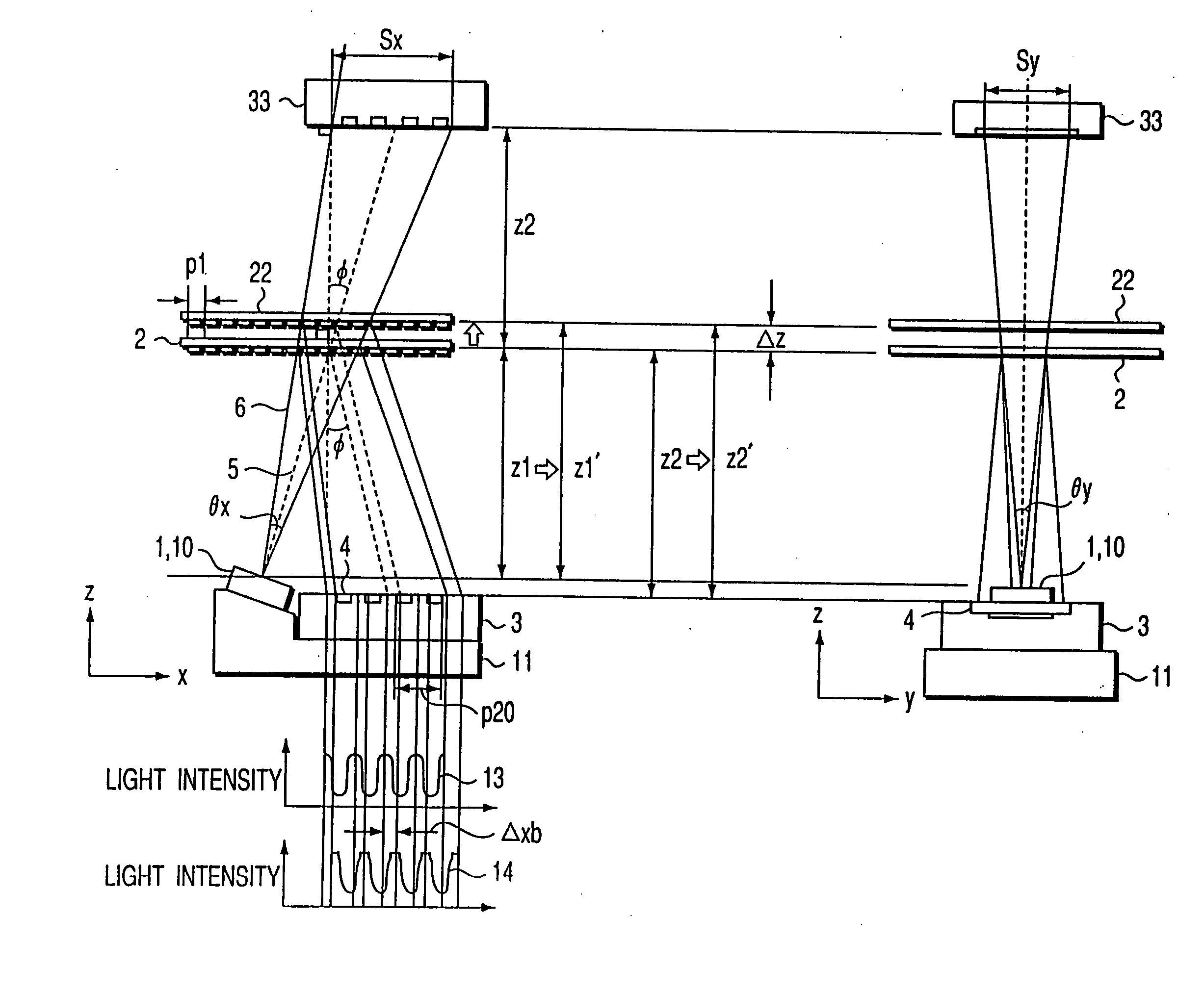
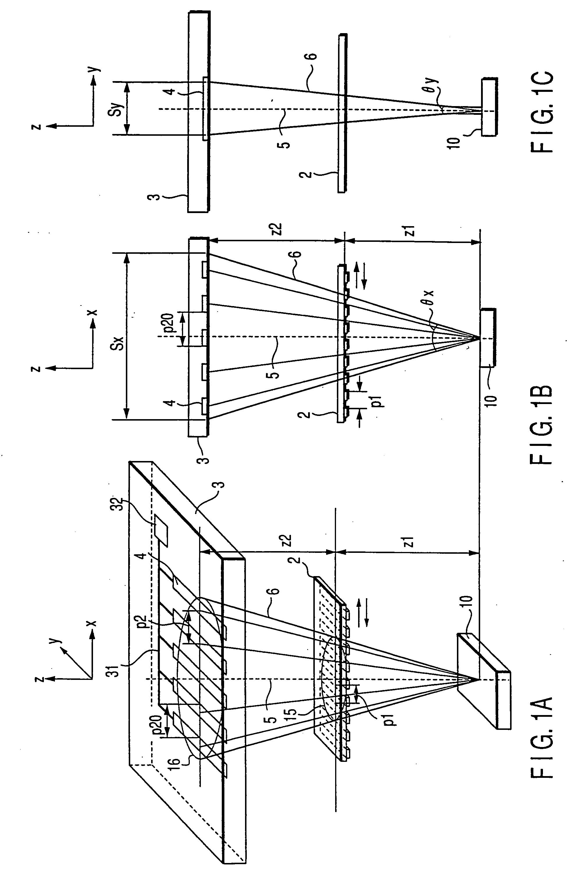
[0192]FIGS. 1A to 1C illustrate the schematic structure of an optical displacement sensor according to a first embodiment of this invention. FIG. 1A is a perspective view showing the structure of the first embodiment, FIG. 1B is a cross-sectional view of an xz plane corresponding to FIG. 1A and FIG. 1C is a cross-sectional view of a yz plane corresponding to in FIG. 1A.

[0193] As shown in FIGS. 1A to 1C, a surface emitting laser light source 10 and a scale 2 are arranged with such a positional relationship that the light beam emitted from this light source 10 is irradiated on the scale 2, and a photosensor 3 is located so as to receive a predetermined portion of a diffraction interference pattern formed from the light source by the scale 2.

[0194] An area 4 in FIGS. 1A to 1C indicates a light receiving area where the photosensor 3 is so located as to receive a predetermined portion of the diffraction interference pattern. If a plurality of light receiving areas 4 are provided, the l...

second embodiment

[0214] An optical displacement sensor according to a second embodiment of this invention will now be described with reference to FIGS. 6A and 6B.

[0215]FIG. 6A is a perspective view showing the optical displacement sensor according to the second embodiment, and FIG. 6B is a plan view showing the light receiving surface of the photosensor 3 in FIG. 6A as viewed towards the −z direction.

[0216] For those portions which are common to those of the first embodiment, their description will partly be omitted below.

[0217] In addition to the light intensity detecting means that is comprised of a plurality of light receiving areas formed at intervals of p2=np1(z1+z2) / z1, the aforementioned second light intensity detecting means is formed with a light receiving width of pm=mp1(z1+z2) / z1 (where m is a natural number different from n) in the pitch direction of the diffraction interference pattern on the light receiving surface, and those light intensity detecting means are connected to an outpu...

third embodiment

[0224] An optical displacement sensor according to a third embodiment of this invention will now be described with reference to FIG. 7.

[0225]FIG. 7 is a plan view of the light receiving surface of the photosensor 3 in FIG. 6A as viewed towards the −z direction.

[0226] For those portions which are common to those of the second embodiment, their description will be partly omitted below.

[0227] There are two sets of light intensity detecting means which are each comprised of a plurality of light receiving areas formed at intervals of p2=np1(z1+z2) / z1 and are connected to output pads 32 and 33 via the wirings 31.

[0228] The two groups of light receiving areas are shifted from each other by δp20 in the x direction on the light receiving surface.

[0229] The operation of the third embodiment of this invention will now be described.

[0230] When the scale 2 is displaced in the pitch direction, electric signals of different phases are output from the output pads 32 and 33.

[0231] Using the p...


PUM


Abstract

An optical displacement sensor comprises a surface emitting laser light source, a scale and a photosensor. The surface emitting laser light source emits a light beam having a predetermined shape. The scale is displaceable in such a manner as to cross the light beam emitted from the surface emitting laser light source and has a diffraction grating of a predetermined period formed thereon for forming a diffraction interference pattern from the light beam. The photosensor receives a predetermined portion of the diffraction interference pattern. The photosensor includes light intensity detecting means comprised of a plurality of light receiving areas arranged apart from one another in a pitch direction of the diffraction interference pattern on a light receiving surface at intervals of np1(z1+z2)/z1 where z1 is a distance between a light-beam emitting surface of the surface emitting laser light source and a surface on which the diffraction grating is formed, z2 is a distance between the surface on which the diffraction grating is formed and the light receiving surface of the photosensor, p1 is the pitch of the diffraction grating on the scale, and n is a natural number.

Description

CROSS-REFERENCE TO RELATED APPLICATIONS [0001] The present application is a Continuation Application of U.S. application Ser. No. 09 / 480,506, which is based upon and claims the benefit of priority from the prior Japanese Patent Applications No. 11-006411, filed Jan. 13, 1999, and No. 11-362940, filed Dec. 21, 1999. The entire contents of parent application Ser. No. 09 / 480,506 are incorporated herein by reference.BACKGROUND OF THE INVENTION [0002] The present invention relates to an optical displacement sensor and an optical encoder and, more particularly, to an optical displacement sensor for detecting the displaced amount of a precision mechanism. [0003] The general structure of an encoder, which is a typical conventional displacement sensor as a first prior art, will be described first. FIG. 28 shows the structure of a conventional laser encoder using a coherent light source and a diffraction grating scale as an example of a miniaturized low cost encoder that does not require asse...

Claims


Application Information

Patent Timeline
Patent Type & Authority Applications(United States)
IPC IPC(8): G01D5/38H03M1/30
CPCH03M1/301G01D5/38
Inventor YAMAMOTO, EIJIHANE, JUNKOMAZAKI, IWAO
Owner OLYMPUS CORP
Why Eureka
Try Eureka