Methods and apparatus for forming thin films for semiconductor devices

Active Publication Date: 2005-07-21
SAMSUNG ELECTRONICS CO LTD
View PDF5 Cites 10 Cited by
  • Summary
  • Abstract
  • Description
  • Claims
  • Application Information

AI Technical Summary

Benefits of technology

[0014] Exemplary embodiments of the invention generally include methods and apparatus for forming thin films for semiconductor devices, which enable the supply amount of a reactant to be increased by preheating and supplying a process gas used to bubble the reactant to a certain temperature so that a heating effect of

Problems solved by technology

However, the use of a typical chemical vapor deposition (CVD) method, a typical physical vapor deposition (PVD) method, or the like in the formation of the thin film makes it difficult to achieve excellent step coverage.
In the typical CVD method, a deposition process utilizing a surface kinetic mode allows the dielectric film having relatively excellent step coverage to be obtained, but since reactants needed to deposit the dielectric film are simultaneously delivered onto a substrate, it is difficult to adjust the step coverag

Method used


Image

  • Methods and apparatus for forming thin films for semiconductor devices
  • Methods and apparatus for forming thin films for semiconductor devices
  • Methods and apparatus for forming thin films for semiconductor devices

Examples


Embodiment Construction

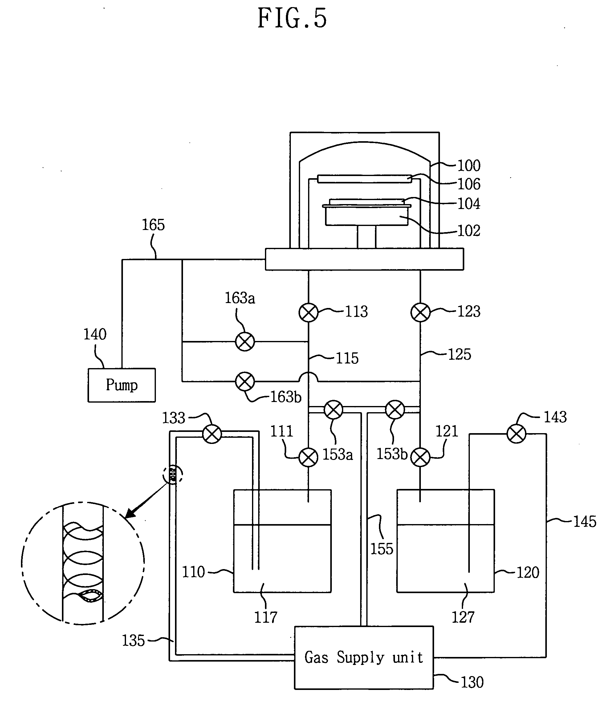
[0029]FIG. 5 schematically illustrates an apparatus for forming a thin film for a semiconductor device according to an exemplary embodiment of the present invention. The structure of a thin film forming apparatus, and a thin film forming method according to an exemplary embodiment of the present invention will be discussed with reference to FIG. 5.

[0030] First, the structure of the thin film forming apparatus according to an exemplary embodiment of the present invention will be described with reference to FIG. 5. The apparatus includes a chamber 100 into which a substrate is loaded, a first reactant supply unit 110 for supplying a first reactant to the chamber, a second reactant supply unit 120 for supplying a second reactant to the chamber, a gas supply unit 130 for supplying a process gas to the chamber 100, the first reactant supply unit 110 and the second reactant supply unit 120, and a pump 140 for performing a pumping operation to remove remaining residues in the chamber. The...


PUM

PropertyMeasurementUnit
Temperatureaaaaaaaaaa
Shapeaaaaaaaaaa

Abstract

Methods and apparatus are provided for forming thin films for semiconductor devices, which enable supplying and removing reactants containing constituent elements of a thin film to be formed, by preheating and supplying a process gas and a purging gas at a predetermined temperature in forming the thin film on a substrate. For example, a method for forming a thin film includes supplying a first reactant to a chamber to chemically adsorb the first reactant onto a substrate, the first reactant being bubbled by a first gas that is preheated, purging the chamber to remove residues on the substrate having the first reactant chemically adsorbed, and forming the thin film by a means of chemical displacement by supplying a second reactant to the chamber to chemically adsorb the second reactant onto the substrate.

Description

CROSS-REFERENCE TO RELATED APPLICATION [0001] This application claims priority to Korean Patent Application No. 2004-4212, filed Jan. 20, 2004, which is incorporated herein by reference in its entirety. TECHNICAL FIELD OF THE INVENTION [0002] The present invention relates, generally, to semiconductor fabrication and, more particularly, to methods and apparatus for forming thin films for semiconductor, devices using atomic layer deposition (ALD). BACKGROUND [0003] Generally, a thin film is used as, for example, a dielectric film of a semiconductor device, a transparent conductor of a liquid crystal display device, a protection layer of an electroluminescent thin film display, and the like. In particular, when the thin film is used as the dielectric film of the semiconductor device, it is required to have no impurity or defect in the dielectric film and at an interface of the dielectric film to secure high capacitance and suppress current leakage. Further, a thin film must have excell...

Claims


Application Information

Patent Timeline
IPC IPC(8): H01L21/205H01L21/285H01L21/314H01L21/316
CPCH01L21/28562H01L21/3141H01L21/31604H01L21/31691H01L21/31641H01L21/31645H01L21/31637H01L21/0228H01L21/02183H01L21/02189H01L21/02181H01L21/02263H01L21/02197H01L21/205C23C16/44
Inventor YEO, JAE-HYUNPARK, YOUNG-WOOKKIM, KI-CHULHAN, JAE-JONG
Owner SAMSUNG ELECTRONICS CO LTD
Why Eureka
Try Eureka