Low injection charge pump

a charge pump and low-injection technology, applied in electronic switching, pulse automatic control, pulse technique, etc., can solve the problems of pulses, dead-band in the pll response, and no down , so as to reduce current overshoot and transistor turn-off slowness, fast switching response, and reduce the effect of effected nois

Inactive Publication Date: 2005-07-28
MICRON TECH INC
View PDF12 Cites 11 Cited by
  • Summary
  • Abstract
  • Description
  • Claims
  • Application Information

AI Technical Summary

Benefits of technology

[0008] The present invention provides a charge pump which has a fast switching characteristic and which mitigates the effected noise, current overshoot and transistor turn-off slowness at the charge pump output. The invention also provides a PLL or DLL circuit which uses the charge pump.
[0009] The charge pump incorporates n-channel and p-channel switching transistors and n-channel and p-channel biasing transistors, as well as a capacitive coupling of complementary versions of the signals used to switch the n-channel and p-channel switching transistors to respective nodes which interconnect the p-channel switching and biasing transistors and the n-channel switching and biasing transistors. The capacitively coupled complementary signals cause the charge pump to maintain a fast switching response without output waveform distortion.

Problems solved by technology

One problem with charge pump 11 is that with real world transistor devices and process spreads, when the PLL is in lock, neither the UP 15 nor the DOWN 17 pulses occur.
This causes a dead-band in the PLL response where differences in phase between an applied system clock signal SYCLK and a PLL generated clock signal CPU cannot be detected.
However, there is a problem in producing a very short pulse at the output of charge pump 11, as it requires a very fast turn on and turn off of the charge pump 11 without a large amount of charge coupling which might distort the output signal.

Method used


Image

  • Low injection charge pump
  • Low injection charge pump
  • Low injection charge pump

Examples


Embodiment Construction

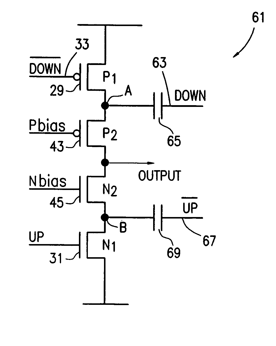
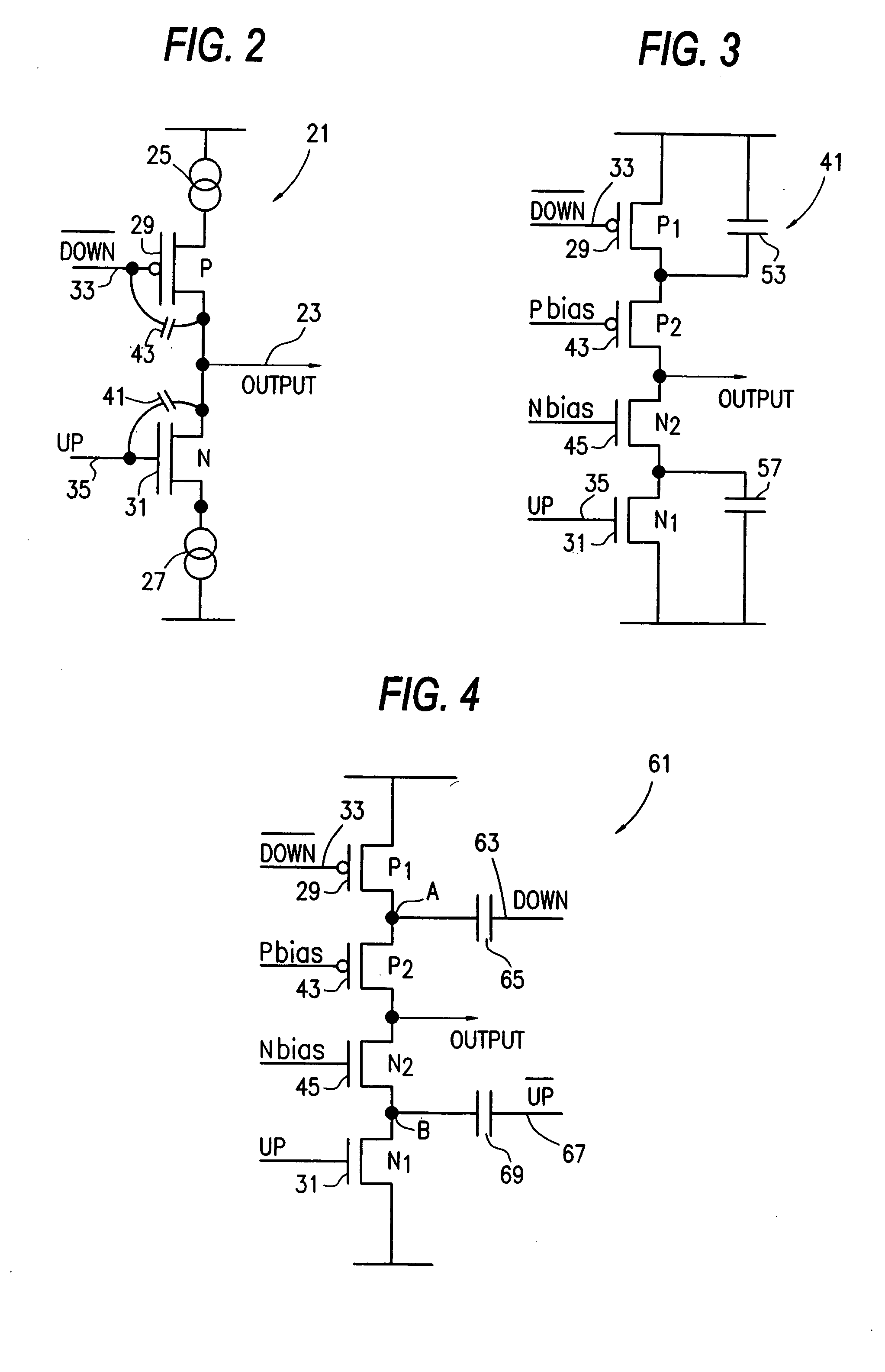
[0019]FIG. 4 illustrates an exemplary embodiment of a CMOS charge pump 61 in accordance with the invention. The circuit is essentially the same as that illustrated in FIG. 3, except for the addition of coupling capacitors 65 and 69 which respectively receive an inverted form of the {overscore (DOWN)} signal applied to gate 33, that is a DOWN signal, and capacitor 69 which receives an inverted form of the UP signal, that is an {overscore (UP)} signal.

[0020] The signal DOWN is applied through capacitor 65 to the common node A of respective switching and D.C. biasing transistors 29 and 43, while the switching signal {overscore (UP)} is applied through capacitor 69 to the common node 13 between respective transistors 45 and 31. The provision of the switching signals DOWN and UP to respective nodes A and B provides a fast turn on and turn off of the transistors 29 and 31 without waveform distortion in the resulting output signal. The voltage on the capacitors 65 and 69 settles to a DC p...


PUM


Abstract

A fast acting charge pump is provided which is suitable for use in a locked loop circuit where very short duration first and second adjustment pulses are produced by a phase detector. The first complement of the second adjustment pulses are used to switch the output of the charge pump through respective pairs of switching and associated biasing transistors, while a complement of the first and second adjustment pulses are respectively capacitively coupled to interconnection nodes of the pairs of switching and biasing transistors.

Description

[0001] The present invention relates to charge pumps which have particular utility in phase lock loop (PLL) and delay lock loop (DLL) circuits. DISCUSSION OF THE RELATED ART [0002] Phase lock loop and delay lock loop circuits are widely used for frequency multiplication and to produce precise delay signals from an incoming clock signal. When such circuits are used in high speed environments such as serial communications, they often need very low phase offset between input and output signals. One common PLL architecture is shown in FIG. 1 and is described in greater detail in the article “A Wide-Bandwidth Low-Voltage PLL for Power PC” Microprocessors” by Alvarez et al., Journal of Solid-State Circuits, Vol. 30, No. 4 Apr. 1995. The entire contents of this article are incorporated herein by reference. The PLL of FIG. 1 relies on a charge pump 11 which receives UP 15 and DOWN 17 pulse signals from a phase detector 13 with the output of the charge pump 11 feeding a PLL loop integrating ...

Claims


Application Information

Patent Timeline
Patent Type & Authority Applications(United States)
IPC IPC(8): H03L7/089H03L7/18
CPCH03L7/18H03L7/0896
Inventor LEVER, ANDREW M.
Owner MICRON TECH INC
Why Eureka
Try Eureka