Vertical nanotube semiconductor device structures and methods of forming the same

a technology of vertical fet devices and semiconductor devices, which is applied in the field of vertical fet device structures, can solve the problems of large variation in current flowing from the source to the drain, and the method of forming such horizontal fet device structures is incompatible with mass production techniques

Inactive Publication Date: 2005-08-04
GLOBALFOUNDRIES INC
View PDF20 Cites 86 Cited by
  • Summary
  • Abstract
  • Description
  • Claims
  • Application Information

AI Technical Summary

Benefits of technology

[0008] Each semiconducting nanotube defines a channel region of a field effect transistor having a channel regulated by application of a control voltage to the gate electrode. Consistent with the principles of the invention, the length of the channel region between the source and drain is defined by the vertical dimension or thickness of the gate electrode without the limitations imposed by conventional lithographic processes used in semiconductor device fabrication to form channel regions in conventional field effect transistors.

Problems solved by technology

A small change in gate voltage can cause a large variation in the current flowing from the source to the drain.
However, these methods of forming such horizontal FET device structures are incompatible with mass production techniques.

Method used


Image

  • Vertical nanotube semiconductor device structures and methods of forming the same
  • Vertical nanotube semiconductor device structures and methods of forming the same
  • Vertical nanotube semiconductor device structures and methods of forming the same

Examples


Embodiment Construction

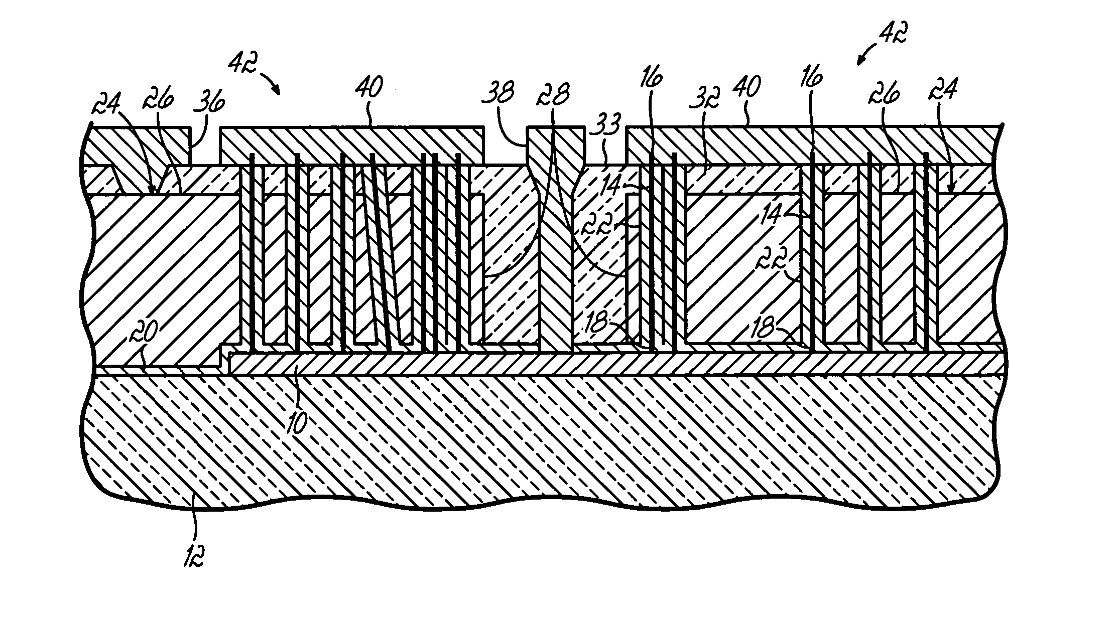
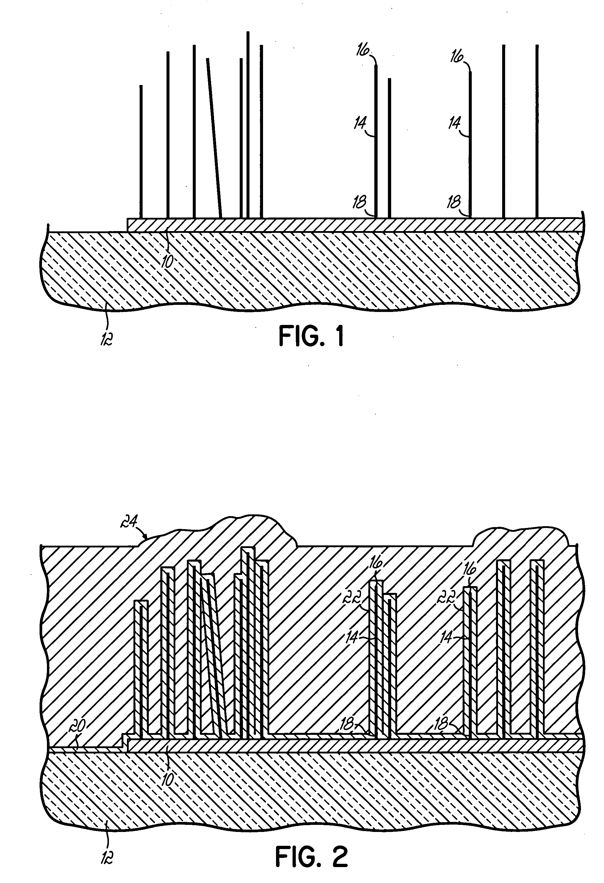
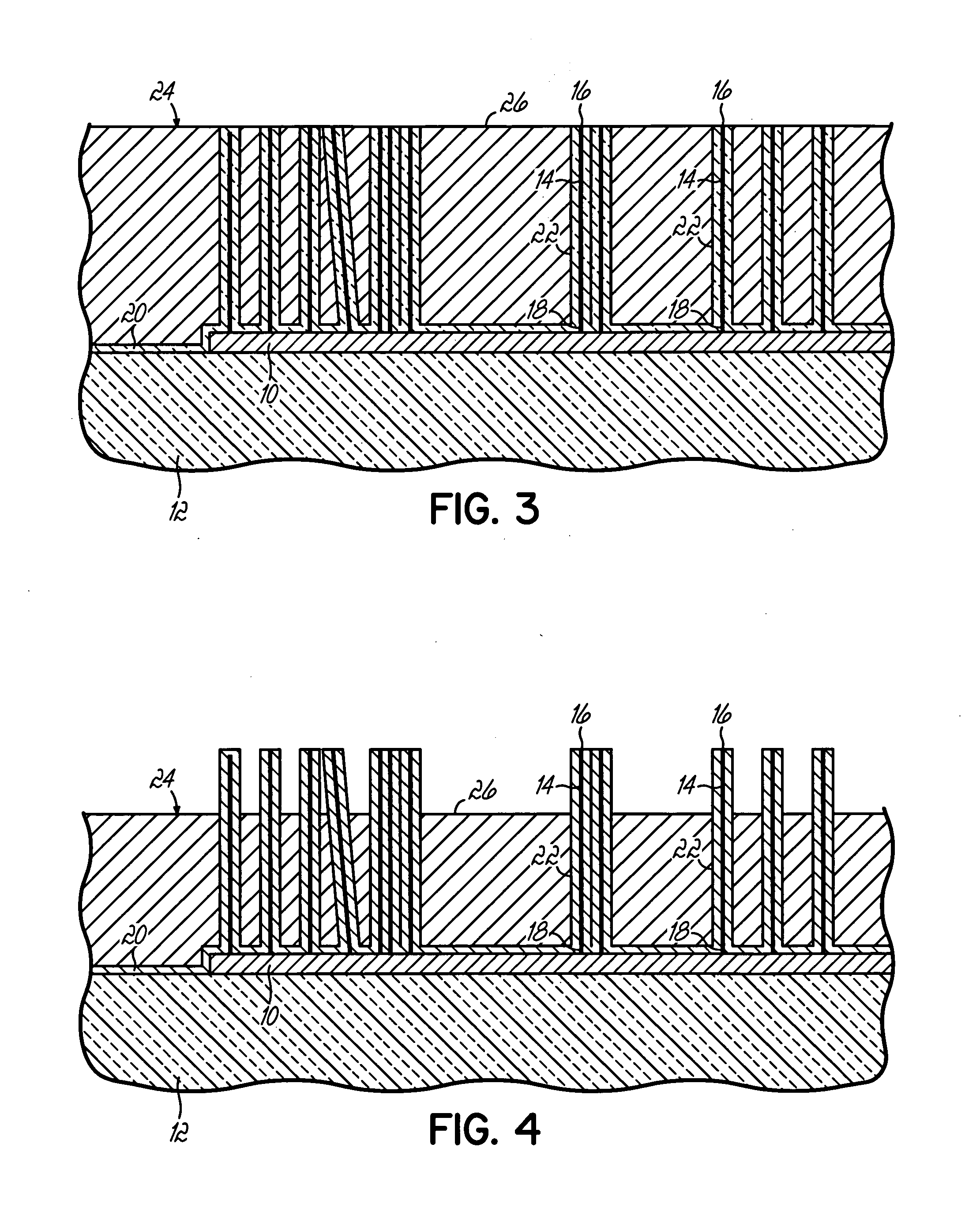
[0022] The invention is directed to vertical field effect transistors (FET's) that utilize carbon nanotubes as a semiconducting material for the channel region providing a selective conduction path between a source and a drain when a voltage is applied to an electrostatically-coupled gate electrode. In accordance with the principles of the invention, the length of the channel region between the source and drain is defined by the thickness of the gate electrode, which is substantially equal to the nanotube length, and is not dependent upon a resolution-limited lithographic process. The carbon nanotubes do not have to be individually manipulated for placement between a source and a drain nor does device fabrication depend upon coincidental alignment with the source and drain of one or more nanotubes randomly dispersed on the device surface.

[0023] With reference to FIG. 1, a catalyst pad 10 of a catalytic material suitable for supporting the growth of carbon nanotubes 14 is formed as ...


PUM

PropertyMeasurementUnit
thicknessaaaaaaaaaa
thicknessaaaaaaaaaa
semiconductingaaaaaaaaaa

Abstract

Vertical device structures incorporating at least one nanotube and methods for fabricating such device structures by chemical vapor deposition. Each nanotube is grown by chemical vapor deposition catalyzed by a catalyst pad and encased in a coating of a dielectric material. Vertical field effect transistors may be fashioned by forming a gate electrode about the encased nanotubes such that the encased nanotubes extend vertically through the thickness of the gate electrode. Capacitors may be fashioned in which the encased nanotubes and the corresponding catalyst pad bearing the encased nanotubes forms one capacitor plate.

Description

FIELD OF THE INVENTION [0001] The invention relates to semiconductor device fabrication and, more particularly, to vertical semiconductor device structures, such as field effect transistors and capacitors, incorporating nanotubes as a device element and methods of fabricating such vertical semiconductor device structures. BACKGROUND OF THE INVENTION [0002] Traditional field effect transistors (FET's) are familiar conventional devices commonly incorporated as a fundamental building block into the intricate circuitry of integrated circuit (IC) chips. A single IC chip may feature many thousands to millions of FET's, along with other passive components such as resistors and capacitors, interconnected by conductive paths. FET's operate by varying the resistivity of a channel in a channel region separating a source and a drain. Carriers flow from the source to the drain through the channel in proportion to the variation in electrical resistivity. Electrons are responsible for channel cond...

Claims


Application Information

Patent Timeline
Patent Type & Authority Applications(United States)
IPC IPC(8): B82B1/00B82B3/00H01L27/28H01L51/05H01L51/30H01L51/40
CPCB82Y10/00H01L51/0048Y10S977/70Y10S977/742Y10S977/734H01L51/057H10K85/221H10K10/491H01L21/18B82Y40/00
Inventor FURUKAWA, TOSHIHARUHAKEY, MARK CHARLESHOLMES, STEVEN JOHNHORAK, DAVID VACLAVKOBURGER, CHARLES WILLIAM IIIMITCHELL, PETER H.NESBIT, LARRY ALAN
Owner GLOBALFOUNDRIES INC
Why Eureka
Try Eureka