

Optimized photodiode process for improved transfer gate leakage
a photodiode and transfer gate technology, applied in the field of improved photodiodes, can solve the problems of significant drawbacks of conventional cmos image devices, and achieve the effects of reducing leakage, improving photodiode implanting, and good charge transfer characteristics
- Summary
- Abstract
- Description
- Claims
- Application Information
AI Technical Summary
Benefits of technology
Problems solved by technology
Method used
Image

Examples
Embodiment Construction
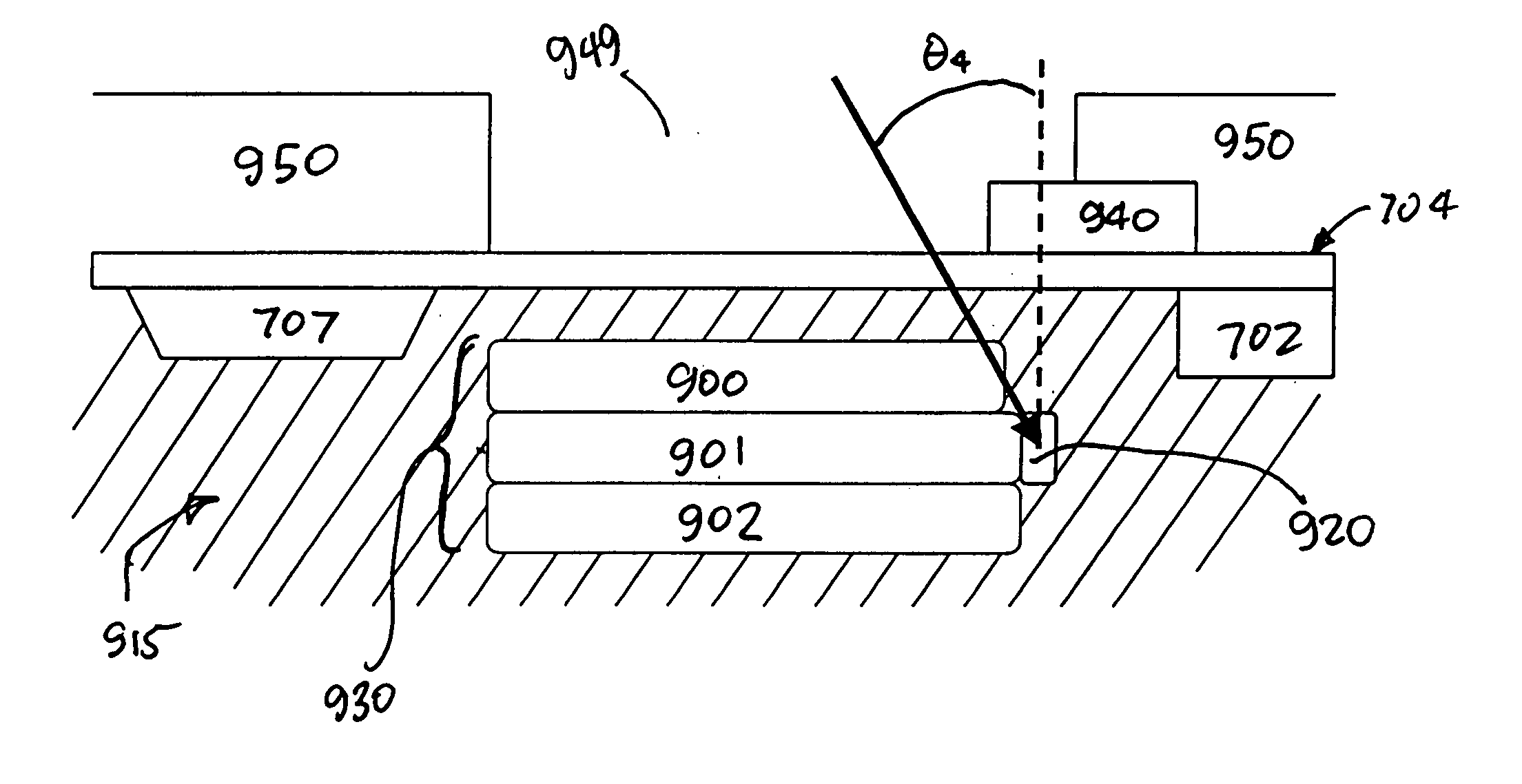
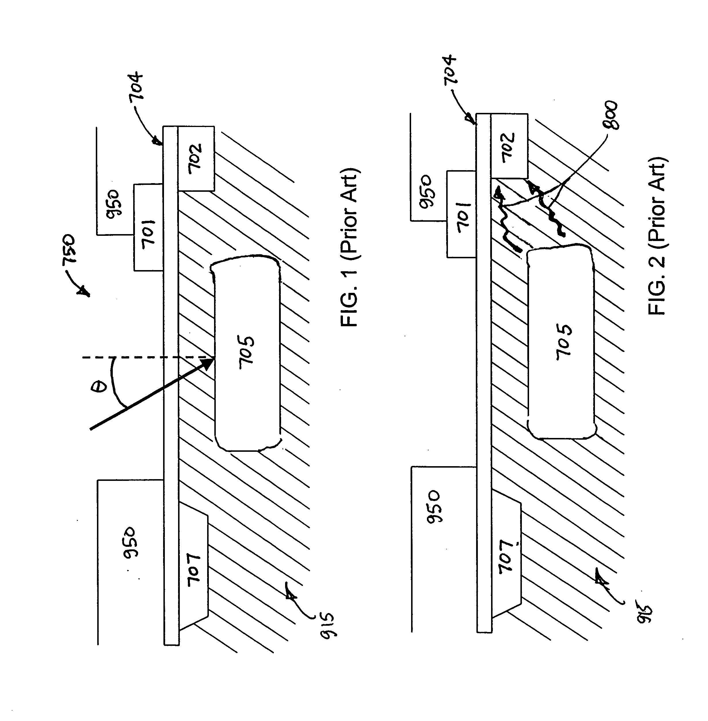
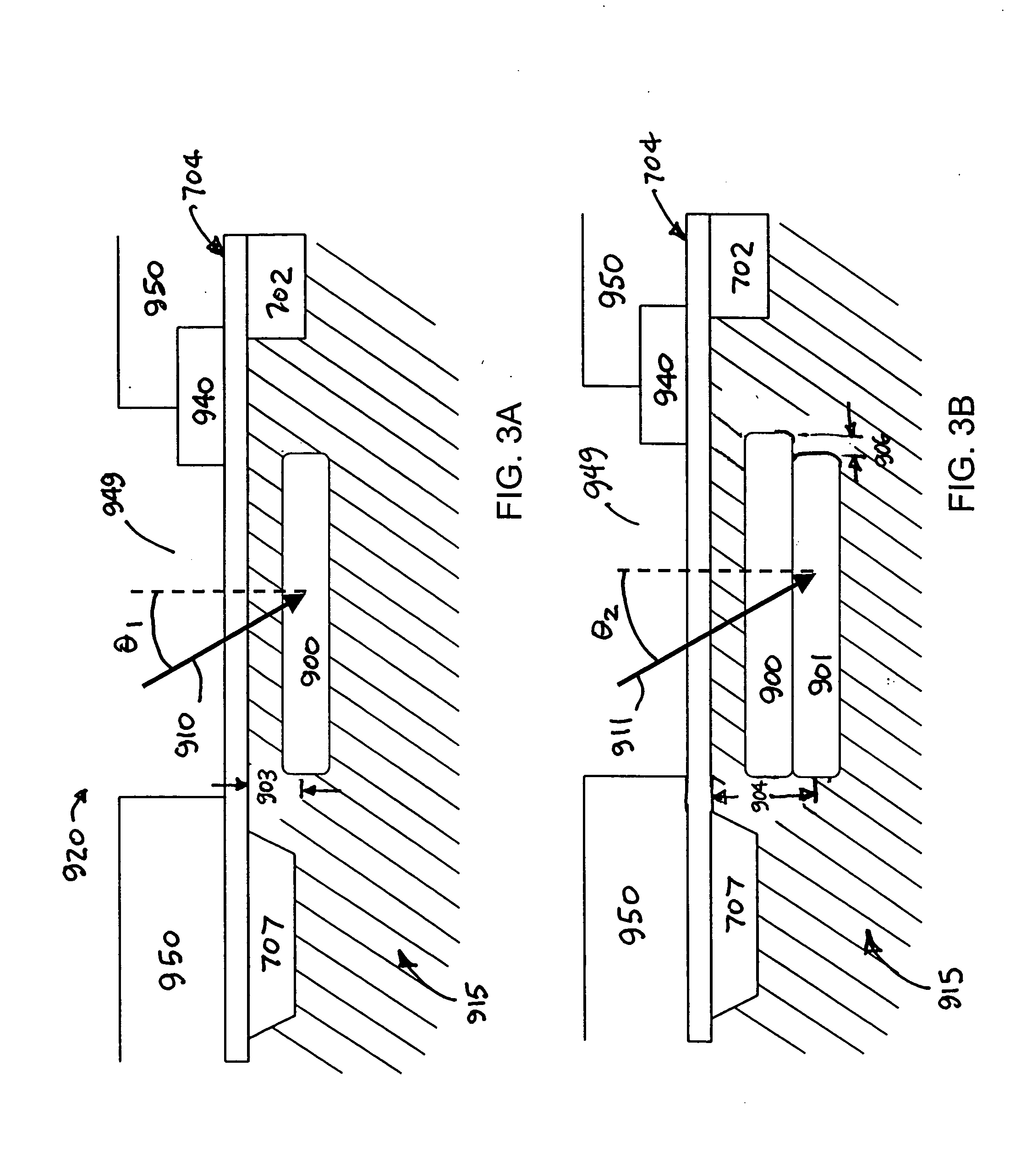
[0019] In the following detailed description, reference is made to the accompanying drawings which form a part hereof, and in which is shown by way of illustration specific embodiments in which the invention may be practiced. These embodiments are described in sufficient detail to enable those skilled in the art to practice the invention, and it is to be understood that other embodiments may be utilized, and that structural, logical and electrical changes may be made without departing from the spirit and scope of the present invention.
[0020] The terms “wafer” and “substrate” are to be understood as including silicon, silicon-on-insulator (SOI) or silicon-on-sapphire (SOS) technology, doped and undoped semiconductors, epitaxial layers of silicon supported by a base semiconductor foundation, and other semiconductor structures. In addition, the semiconductor need not be silicon-based, but could be based on silicon-germanium, germanium, or gallium arsenide. Furthermore, when reference ...
PUM
 Abstract
Description
Claims
Application Information