
Encapsulated spacers in vertical pass gate dram and damascene logic gates

a technology of logic gates and spacers, which is applied in the field of semiconductor devices, can solve the problems of increasing cell leakage, increasing cell leakage, and increasing the size of the device or portions of the device, and achieve the effect of improving the structural integrity of the devi

Inactive Publication Date: 2005-08-04
INFINEON TECH AG +1
View PDF0 Cites 51 Cited by
  • Summary
  • Abstract
  • Description
  • Claims
  • Application Information

AI Technical Summary

Benefits of technology

[0010] The present invention provides devices having enc

Problems solved by technology

However, decreasing the size of the device or portions of the device can have adverse consequences.
The misalignment commonly leads to increased cell leakage caused by leakage between the source and drain regions.
The presence of leakage between source and drain is also a problem for conventional logic chips.
In addition, logic chips also suffer from increased leakage through the gate insulator.
Raised source-drain structures have been proposed to deal with the first problem but usually call for epitaxially growing Si in the source-drain region which is prone to defects.
U.S. Pat. No. 5,998,835 to Furukawa et al. describes a known raised-source drain structure but does not teach encapsulated spacers or damascene gates on the high-K gate dielectrics.

Method used


Image

  • Encapsulated spacers in vertical pass gate dram and damascene logic gates
  • Encapsulated spacers in vertical pass gate dram and damascene logic gates
  • Encapsulated spacers in vertical pass gate dram and damascene logic gates

Examples


Embodiment Construction

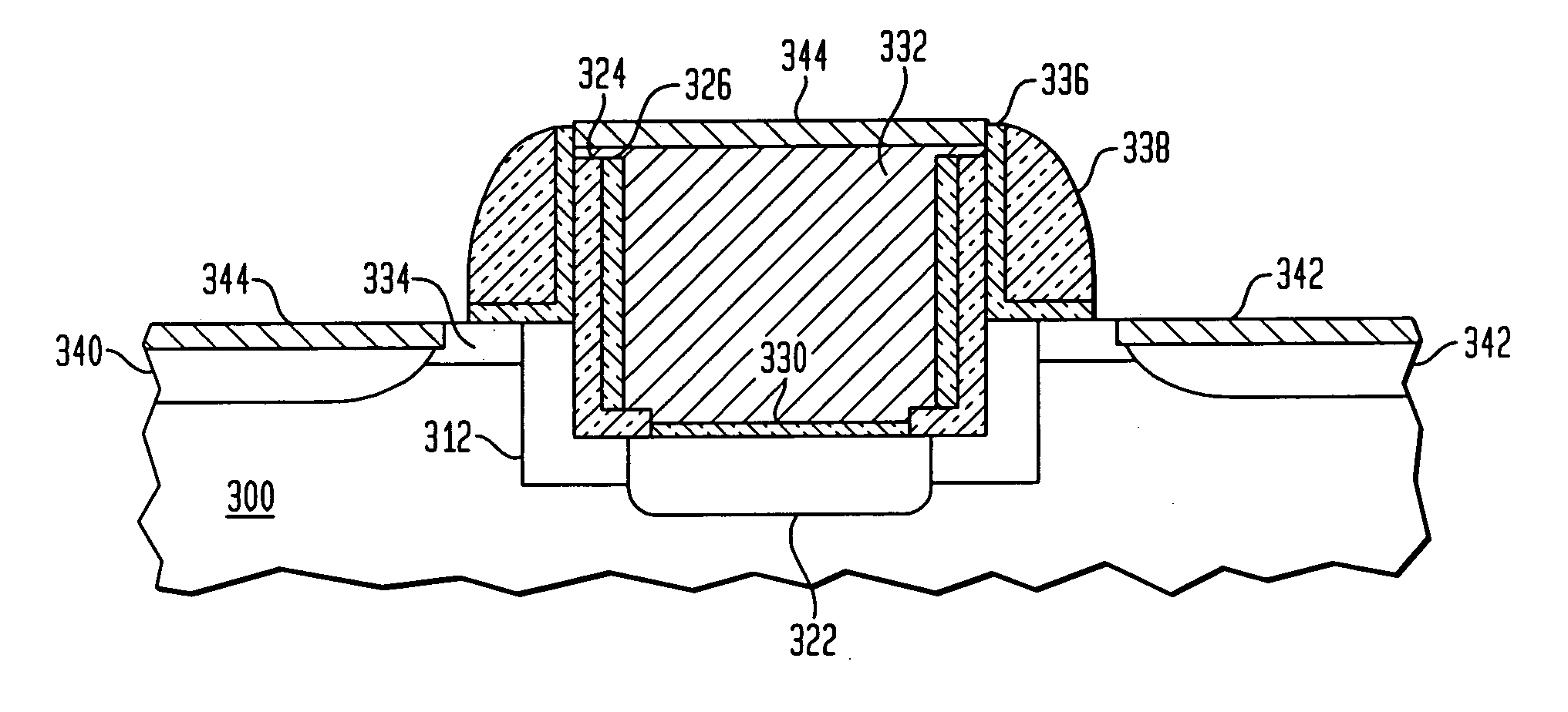
[0024] In accordance with an embodiment of the present invention, a memory cell having improved isolation is provided. The materials and processes described below can be employed with various kinds of substrates including, but not limited to, silicon (Si) and silicon on insulator (SOI). It is to be appreciated that the values of temperature, pressure, time, dimensions, etc. are by way of example only and are approximations that may be varied. It will also be apparent to one of ordinary skill in the art that certain steps may be performed in a different order.

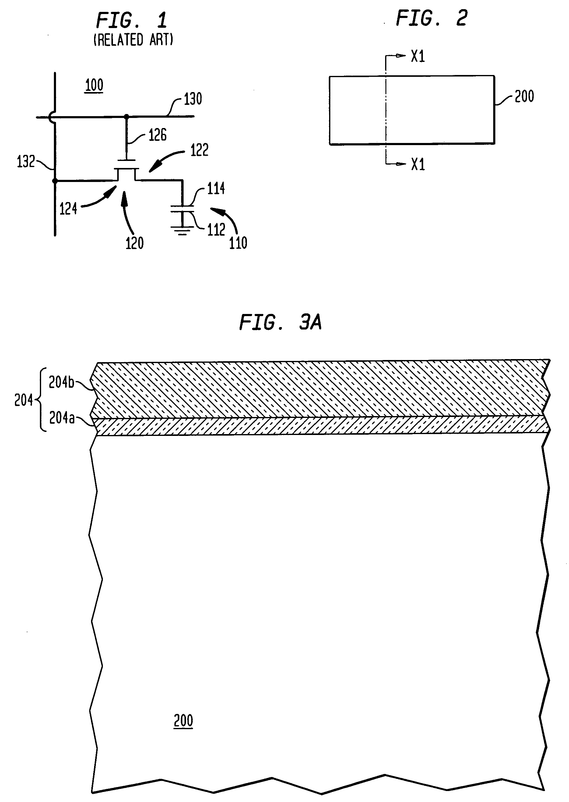
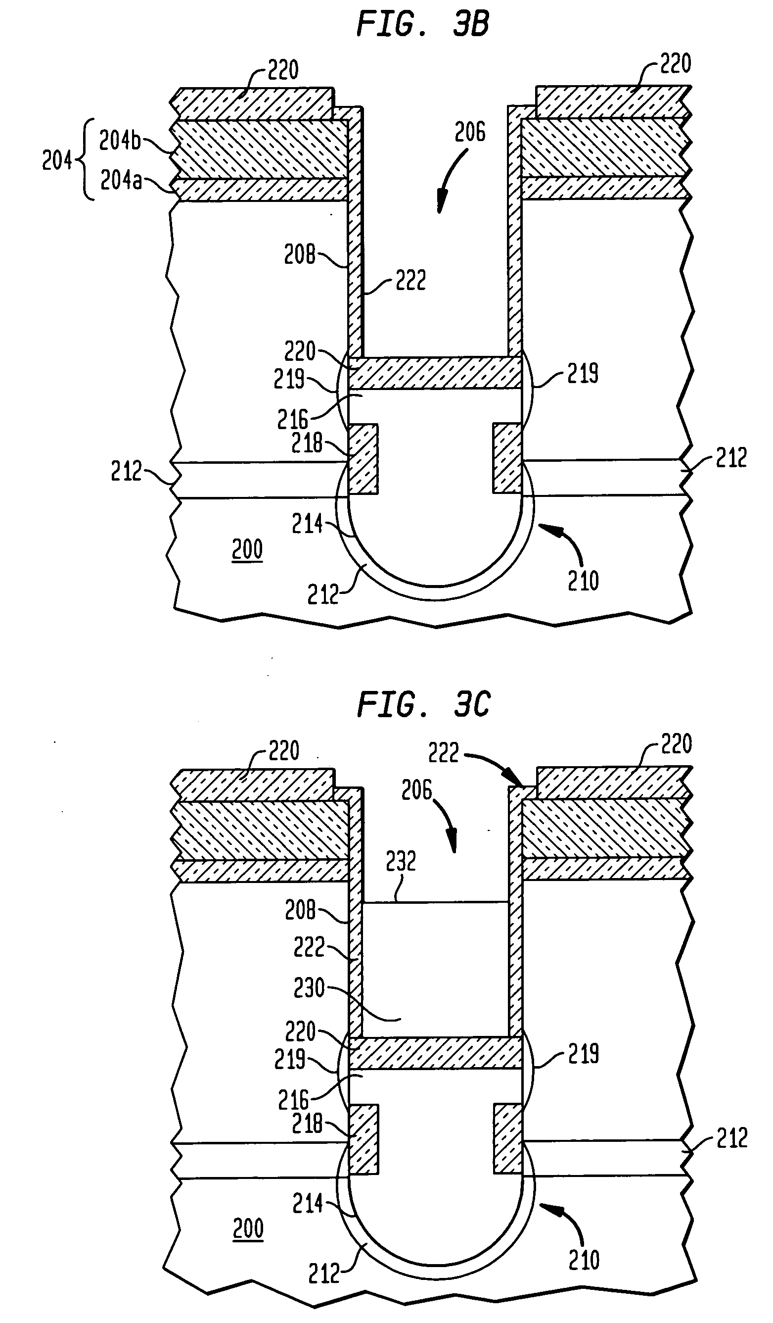
[0025]FIG. 2 is a top view of a part of a memory cell formed in a semiconductor substrate. A process for forming the memory cell is described using cross-sectional views in FIGS. 3A-3H. The cross-sectional views are taken with respect to the line X1-X1 shown in FIG. 2.

[0026]FIG. 3A illustrates a step in a process for fabricating a memory cell in accordance with an aspect of the invention. Disposed on top of a substrate 200 is ...


PUM


Abstract

Semiconductor devices having improved isolation are provided along with methods of fabricating such semiconductor devices. The improved isolation includes an encapsulated spacer formed within a gate region of a device.

Description

BACKGROUND OF THE INVENTION [0001] The present invention relates to semiconductor devices and, more particularly, relates to improved isolation for semiconductor devices. [0002] Semiconductor devices are employed in various systems for a wide range of applications. An important type of semiconductor device is the transistor. Transistors are ubiquitous in electronics and are often used as part of larger devices or systems. For example, transistors may form part of a logic device or may be used to create memory cells such as dynamic random access memory (“DRAM”). [0003] A simple DRAM cell may include one transistor and one capacitor formed on or within a semiconductor substrate. A DRAM cell formed on the semiconductor substrate is known as a stacked memory cell, and a DRAM cell formed within the semiconductor substrate is known as a trench memory cell. The capacitor stores a charge to represent a data value. The transistor allows the data value to be refreshed, read from, or written t...

Claims


Application Information

Patent Timeline
IPC IPC(8): H01L21/28H01L21/336H01L21/8242H01L29/06H01L29/423H01L29/737H01L29/78
CPCH01L21/28114H01L27/10864H01L27/10876H01L27/10891H01L29/0692H01L29/42376H01L29/7834H01L29/66537H01L29/66553H01L29/6656H01L29/6659H01L29/66621H01L29/7371H01L29/665H10B12/0383H10B12/053H10B12/488
Inventor DIVAKARUNI, RAMACHANDRAKUDELKA, STEPHANMANDELMAN, JACK A.
Owner INFINEON TECH AG
Learn More