High-voltage vertical transistor with edge termination structure

a vertical transistor and edge termination technology, applied in the field of field-effect semiconductor transistor structure, can solve the problems of increased production cost, increased on-state resistance, and reduced device on-state performan

Inactive Publication Date: 2005-08-04
POWER INTEGRATIONS INC
View PDF99 Cites 109 Cited by
  • Summary
  • Abstract
  • Description
  • Claims
  • Application Information

AI Technical Summary

Problems solved by technology

The combined decrease in doping and increase in length of the extended drain region therefore have the deleterious effect on the on-state performance of the device, as both cause an increase in on-state resistance.
Another problem associated with conventional HVFET designs is that they usually require a wide perimeter or edge termination area in order to support the large electric fields developed between the various regions.
Naturally, this wide edge termination area uses valuable silicon area leading to increased production costs.

Method used


Image

  • High-voltage vertical transistor with edge termination structure
  • High-voltage vertical transistor with edge termination structure
  • High-voltage vertical transistor with edge termination structure

Examples


Embodiment Construction

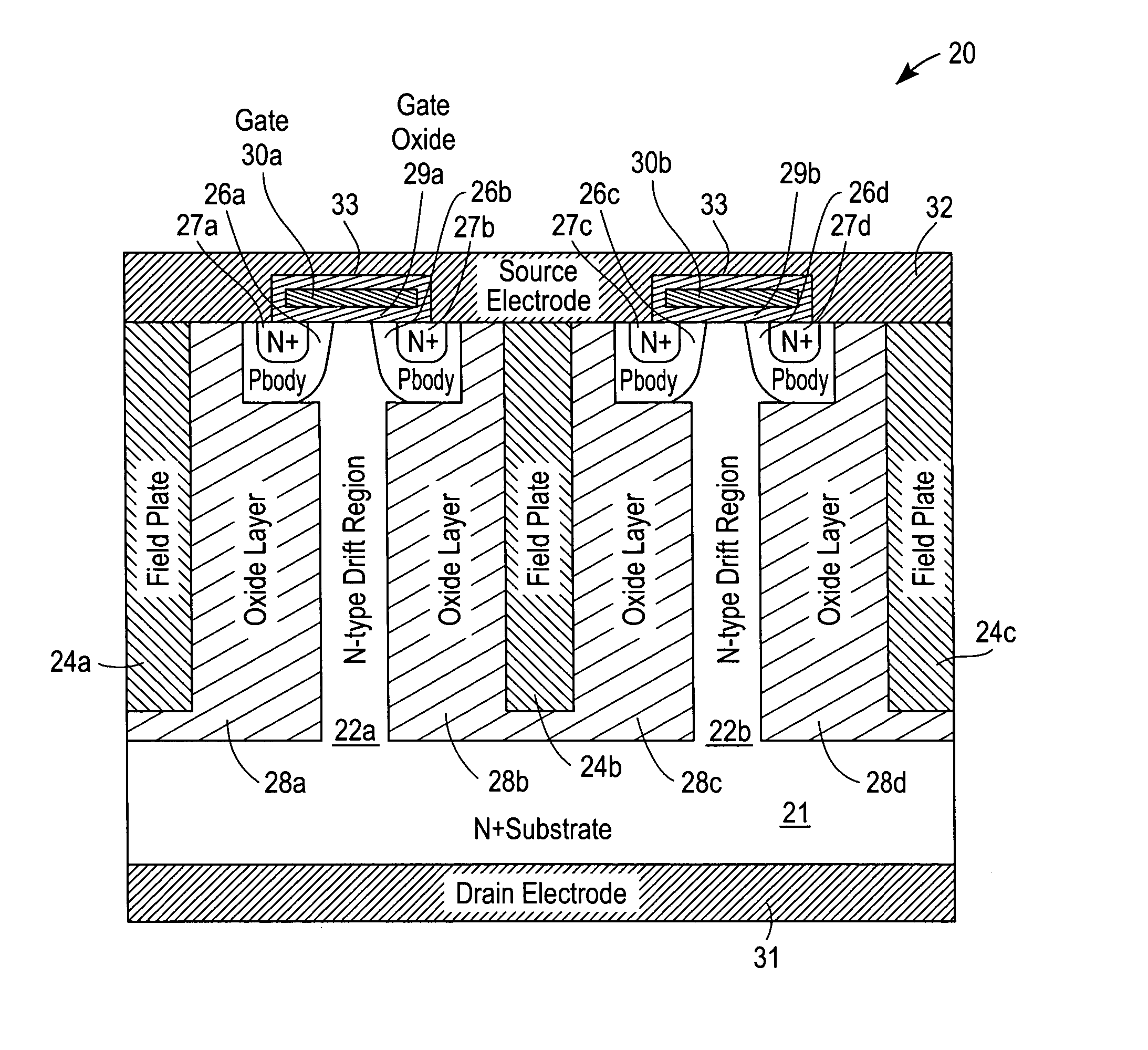
[0023] A high-voltage field-effect transistor (HVFET) having an extended drain or drift region with an edge termination structure is described. The HVFET has a low specific on-state resistance and supports high voltage in the off-state. In the following description, numerous specific details are set forth, such as material types, doping levels, structural features, processing steps, etc., in order to provide a thorough understanding of the present invention. Practitioners having ordinary skill in the semiconductor arts will understand that the invention may be practiced without many of these details. In other instances, well-known elements, techniques, and processing steps have not been described in detail to avoid obscuring the invention.

[0024]FIG. 1 is a cross-sectional side view of a vertical n-channel (i.e., NMOS) HVFET 20 in accordance with one embodiment of the present invention. It should be understood that the elements in the figures are representational, and are not drawn ...


PUM


Abstract

A high-voltage transistor includes a drain, a source, and one or more drift regions extending from the drain toward the source. A field plate member laterally surrounds the drift regions and is insulated from the drift regions by a dielectric layer. It is emphasized that this abstract is provided to comply with the rules requiring an abstract that will allow a searcher or other reader to quickly ascertain the subject matter of the technical disclosure. It is submitted with the understanding that it will not be used to interpret or limit the scope or meaning of the claims. 37 CFR 1.72(b).

Description

RELATED APPLICATIONS [0001] This is a continuation-in-part (CIP) application of application Ser. No. 10 / 393,759 filed Mar. 21, 2003, which is a continuation of Ser. No. 09 / 948,930 filed Sep. 7, 2001, now U.S. Pat. No. 6,573,558, both of which are assigned to the assignee of the present CIP application.FIELD OF THE INVENTION [0002] The present invention relates to semiconductor devices fabricated in a silicon substrate. More specifically, the present invention relates to field-effect semiconductor transistor structures capable of withstanding high voltages. BACKGROUND OF THE INVENTION [0003] High-voltage, field-effect transistors (HVFETs) are well known in the semiconductor arts. Most often, HVFETs comprise a device structure that includes an extended drain region that supports the applied high-voltage when the device is in the “off” state. HVFETs of this type are commonly used in power conversion applications such as AC / DC converters for offline power supplies, motor controls, and s...

Claims


Application Information

Patent Timeline
Patent Type & Authority Applications(United States)
IPC IPC(8): H01L21/336H01L29/06H01L29/40H01L29/417H01L29/423H01L29/78
CPCH01L29/0653H01L29/0696H01L29/402H01L29/407H01L29/41741H01L29/7828H01L29/7802H01L29/7811H01L29/7813H01L29/7824H01L29/42368
Inventor DISNEY, DONALD RAY
Owner POWER INTEGRATIONS INC
Why Eureka
Try Eureka