Semiconductor apparatus and manufacturing method of the same
a technology of semiconductor devices and manufacturing methods, applied in the direction of semiconductor devices, electrical devices, transistors, etc., can solve the problems of parasitic capacity generation, gate insulating film thickness cannot be ignored, and the depletion layer is formed
- Summary
- Abstract
- Description
- Claims
- Application Information
AI Technical Summary
Benefits of technology
Problems solved by technology
Method used
Image

Examples
Embodiment Construction
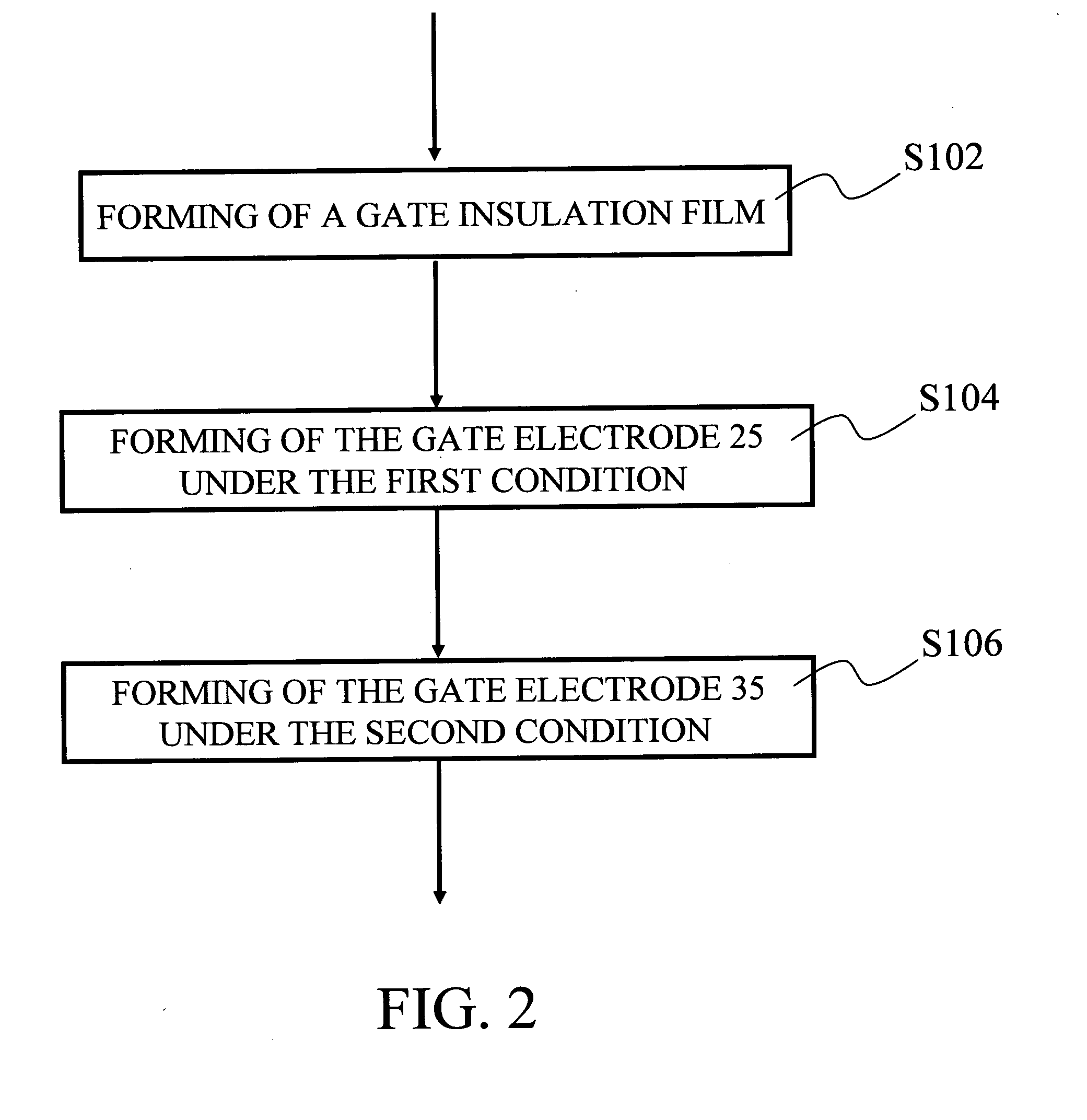
[0030] Hereinafter, the embodiment of the present invention will be explained with reference to the accompanying drawings.
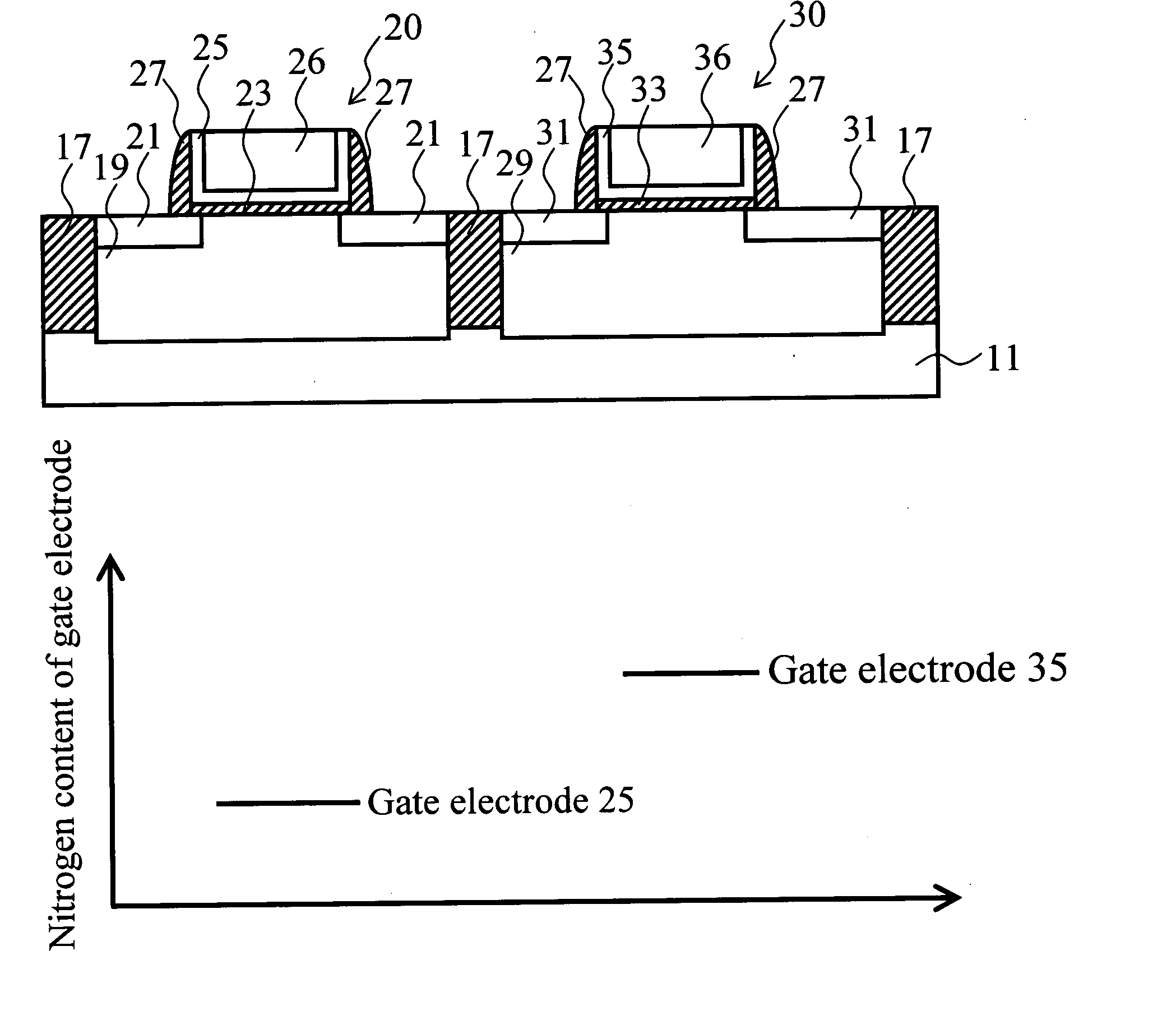
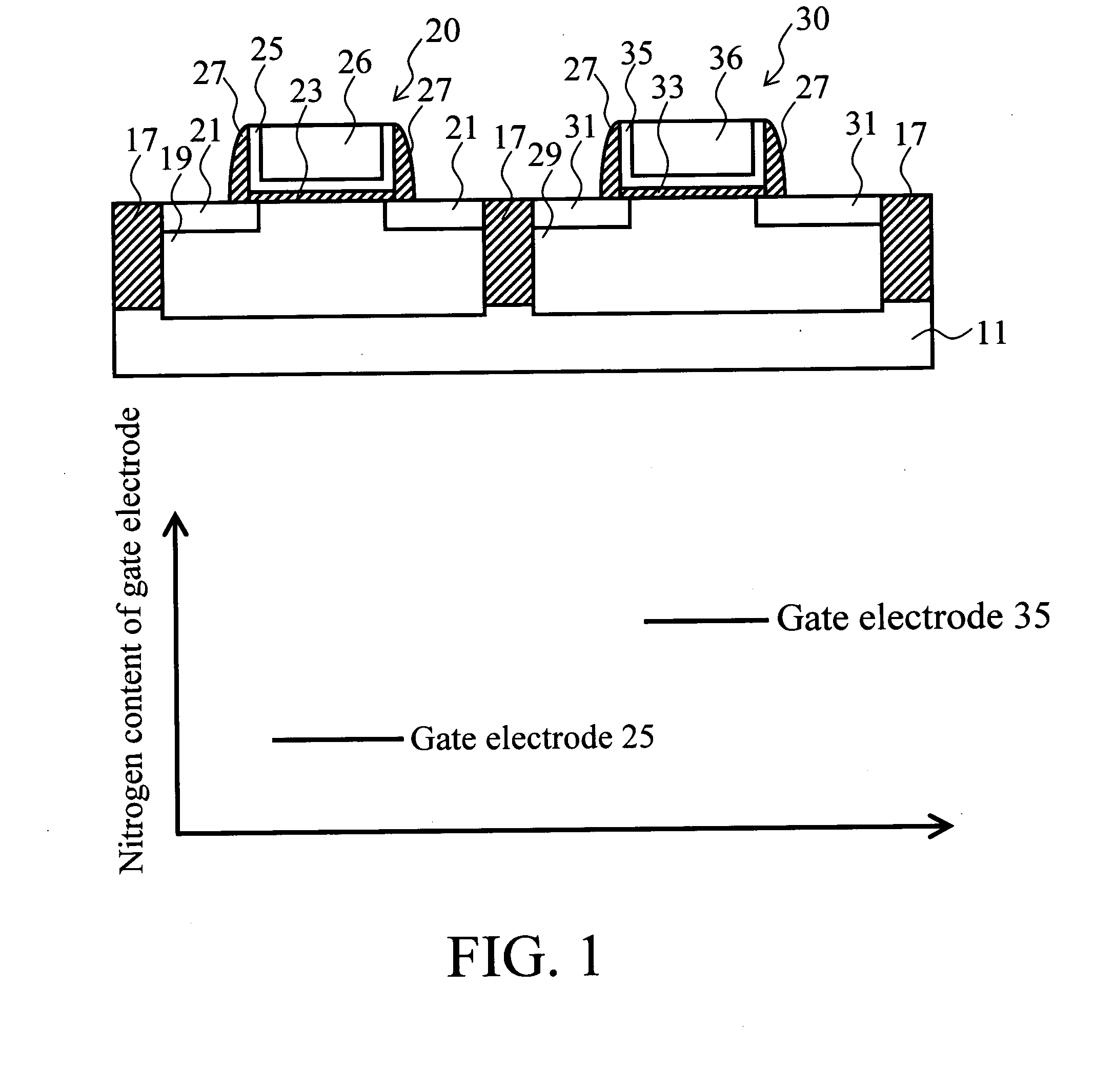
[0031]FIG. 1 is a schematic diagram showing the sectional structure of the essential section of the semiconductor apparatus relating to the embodiment of the present invention. Namely, the drawing is a cross section view of a complementary MISFET of the semiconductor apparatus shown in the drawing having an n-type MISFET (metal-insulator-semiconductor field effect transistor) 20 and a p-type MISFET 30.
[0032] The CMISFET of this embodiment has the n-type MISFET 20 and the p-type MISFET 30 which are formed on the same semiconductor substrate 11. On the surface of the semiconductor substrate 11, between these transistors, for example, an element isolation area 17 formed by embedding an insulating film in a groove is formed.
[0033] The n-type MISFET 20 is formed on a p-type well 19 on the surface of the semiconductor substrate 11. Namely, the n-type MISFET 20 is fo...
PUM
 Abstract
Description
Claims
Application Information
 - Generate Ideas
- Intellectual Property
- Life Sciences
- Materials
- Tech Scout
- Unparalleled Data Quality
- Higher Quality Content
- 60% Fewer Hallucinations
Browse by: Latest US Patents, China's latest patents, Technical Efficacy Thesaurus, Application Domain, Technology Topic, Popular Technical Reports.
© 2025 PatSnap. All rights reserved.Legal|Privacy policy|Modern Slavery Act Transparency Statement|Sitemap|About US| Contact US: help@patsnap.com