Shallow trench isolation structure with converted liner layer

a technology of liner layer and trench isolation, which is applied in the direction of basic electric elements, electrical equipment, semiconductor devices, etc., can solve the problems of hv oxide layer damage, flash memory device especially vulnerable to degradation of production yield, and even failure of adjacent transistors, so as to prevent the formation of dents in the sti structure

Inactive Publication Date: 2005-08-04
SAMSUNG ELECTRONICS CO LTD
View PDF7 Cites 72 Cited by
  • Summary
  • Abstract
  • Description
  • Claims
  • Application Information

AI Technical Summary

Benefits of technology

[0031] In this manner, the liner layer is comprised of the initial material of nitride during the wet etch-back of the first dielectric fill material comprised of oxide. Such a liner layer of nitride protects any oxide layer comprising the masking layers on the semiconductor substrate during the wet etch-back of the first dielectric fill material. Thereafter, the expo

Problems solved by technology

Such dents 38 cause deleterious effects and even failure in an adjacent transistor.
Relative to DRAM or SRAM memory devices, a flash memory device is especially vulnerable to degradation of production yield from formation of such dents 38.
U

Method used


Image

  • Shallow trench isolation structure with converted liner layer
  • Shallow trench isolation structure with converted liner layer
  • Shallow trench isolation structure with converted liner layer

Examples


Embodiment Construction

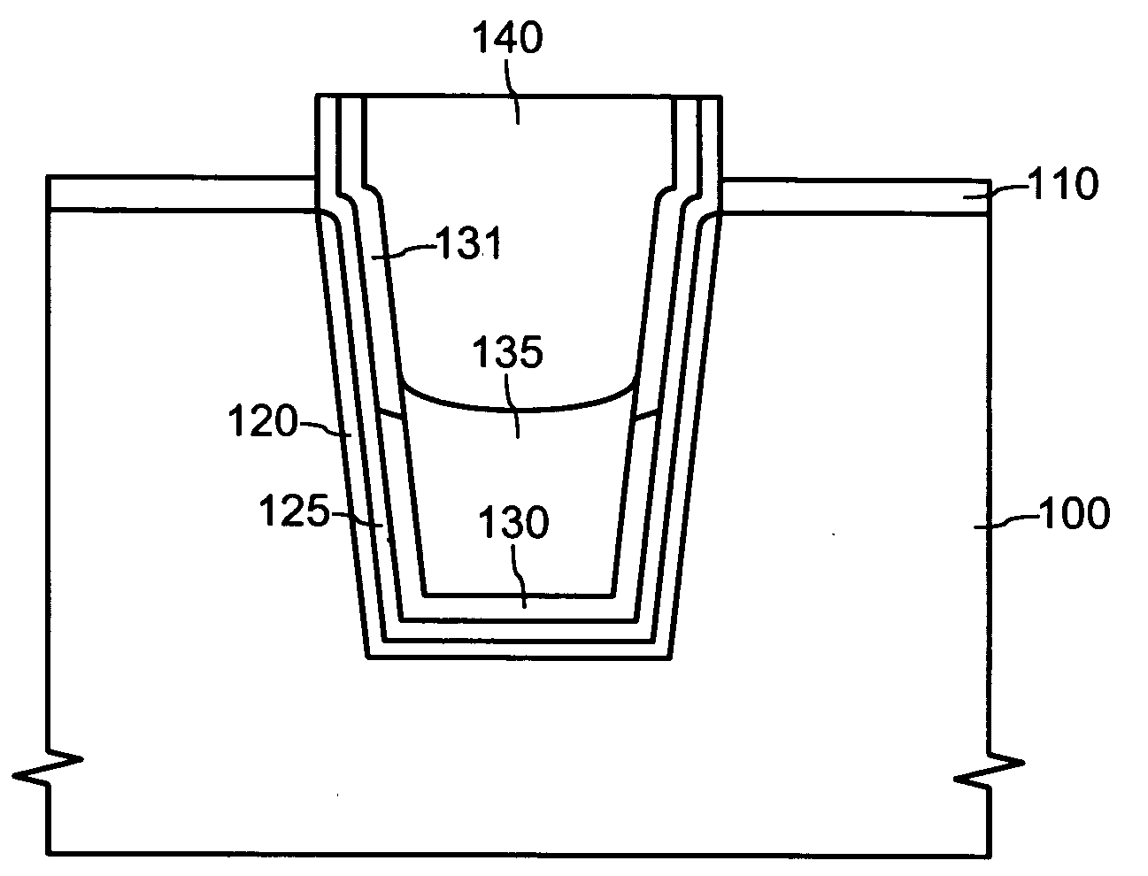
[0039] Referring to FIG. 3, an oxide (SiO2 for example) layer 105 and a nitride (SiN for example) layer 110 form masking layers sequentially formed on a semiconductor substrate 100. The oxide layer 105 and the nitride layer 110 are patterned by a photo etch process to form an opening 102 through such layers 110 and 105. The layers 110 and 105 with the opening 102 form a mask layer pattern 112 for defining an active region on the semiconductor substrate 100.

[0040]FIG. 3 illustrates for example a cell region of a flash memory device or a peripheral circuit region of the flash memory device having the oxide layer 105 as a HV gate oxide layer on the semiconductor substrate 100. Using the mask layer pattern 112 as an etch mask, the semiconductor substrate 100 is anisotropically dry-etched to form a STI opening 102 through the semiconductor substrate 100. The STI opening 102 is formed as a STI trench in one embodiment of the present invention. However, the present invention may be practi...


PUM


Abstract

A STI (shallow trench isolation) structure is formed with a liner layer that is converted from an initial material to a subsequent material. For example, the liner layer is initially comprised of nitride during wet etch-back of a dielectric fill material comprised of oxide to protect an oxide layer on a semiconductor substrate. Thereafter, an exposed portion of the liner layer is converted into the subsequent material of oxide to protect the dielectric fill material within the STI opening during etching away of masking layers to prevent formation of dents in the STI structure.

Description

BACKGROUND OF THE INVENTION [0001] This application claims priority to Korean Patent Application No. 2004-006980, filed on Feb. 3, 2004, in the Korean Intellectual Property Office, the disclosure of which is incorporated herein in its entirety by reference. [0002] 1. Field of the Invention [0003] The present invention relates generally to IC (integrated circuit) fabrication, and more particularly, to a shallow trench isolation (STI) structure with a liner layer that is converted from an initial material to a subsequent material for preserving the integrity of IC structures associated with the STI structure. [0004] 2. Description of the Related Art [0005] Isolation technology is important for electrically isolating adjacent IC (integrated circuit) devices fabricated in a semiconductor substrate, especially with demand for higher integration and capacity of IC devices. Shallow trench isolation (STI) is particularly suited for the fabrication of highly integrated IC devices. [0006] For...

Claims


Application Information

Patent Timeline
IPC IPC(8): H01L21/762
CPCH01L21/76224H01L21/762
Inventor KIM, SHIN-HYEKIM, MINLEE, SEUNG-JAE
Owner SAMSUNG ELECTRONICS CO LTD
Why Eureka
Try Eureka