Semiconductor resistor

a technology of semiconductor resistor and resistor, which is applied in the direction of resistor details, solid-state devices, basic electric elements, etc., can solve the problems of localized heating and electromigration, increase the overall area consumed by the ic device, and complete or partial failure of the metal interconnection line, etc., to achieve uniform current distribution and improve the structure of the semiconductor resistor

Active Publication Date: 2005-08-04
BELL SEMICON LLC
View PDF6 Cites 11 Cited by
  • Summary
  • Abstract
  • Description
  • Claims
  • Application Information

AI Technical Summary

Benefits of technology

[0009] In the illustrative embodiment of the invention, a terminal conductor, which provides electrical connection between the semiconductor resistor and at least one other circuit component and / or structure in an IC device, is configured such that a resistance of the terminal conductor between at least two contacts connecting the terminal conductor to a resistor body portion is substantially matched to a resistance of the resistor body between the at least two contacts. Since current will divide among two or more conductive paths according to the resistance associated with each path, by providing substantially equal resistance paths, the current distribution in the contact paths will also be substantially equal to one another. Thus, electromigration and / or localized heating in the semiconductor resistor is beneficially reduced, without significantly increasing semiconductor area and / or cost.

Problems solved by technology

This unequal current distribution in the semiconductor resistor often results in localized heating and electromigration, particularly in the contact regions of the resistor.
Electromigration is a well-known reliability problem which generally involves the movement of atoms in a metal interconnection line due to momentum transfer from conduction electrons.
The metal atoms migrate in the direction of current flow and can eventually lead to a complete or partial failure of the metal interconnection line.
However, increasing the number of rows of contacts does not solve the inherent unequal current distribution problem in the resistor, and thus a majority of the current will continue to flow through an inner row of the contacts.
Moreover, increasing the dimensions of the semiconductor resistor undesirably increases the overall area consumed by the IC device.

Method used


Image

  • Semiconductor resistor
  • Semiconductor resistor
  • Semiconductor resistor

Examples


Embodiment Construction

[0017] The present invention will be described herein in the context of an illustrative semiconductor resistor structure. It should be understood, however, that the present invention is not limited to this or any particular resistor arrangement. Rather, the invention is more generally applicable to techniques for improving a reliability of a semiconductor resistor by beneficially providing a substantially uniform current distribution in a contact region of the semiconductor resistor.

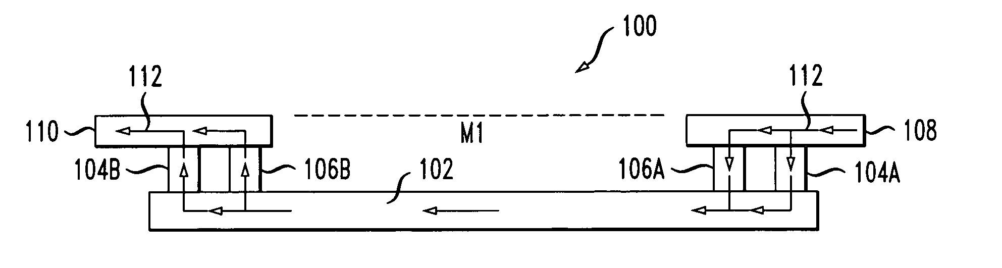
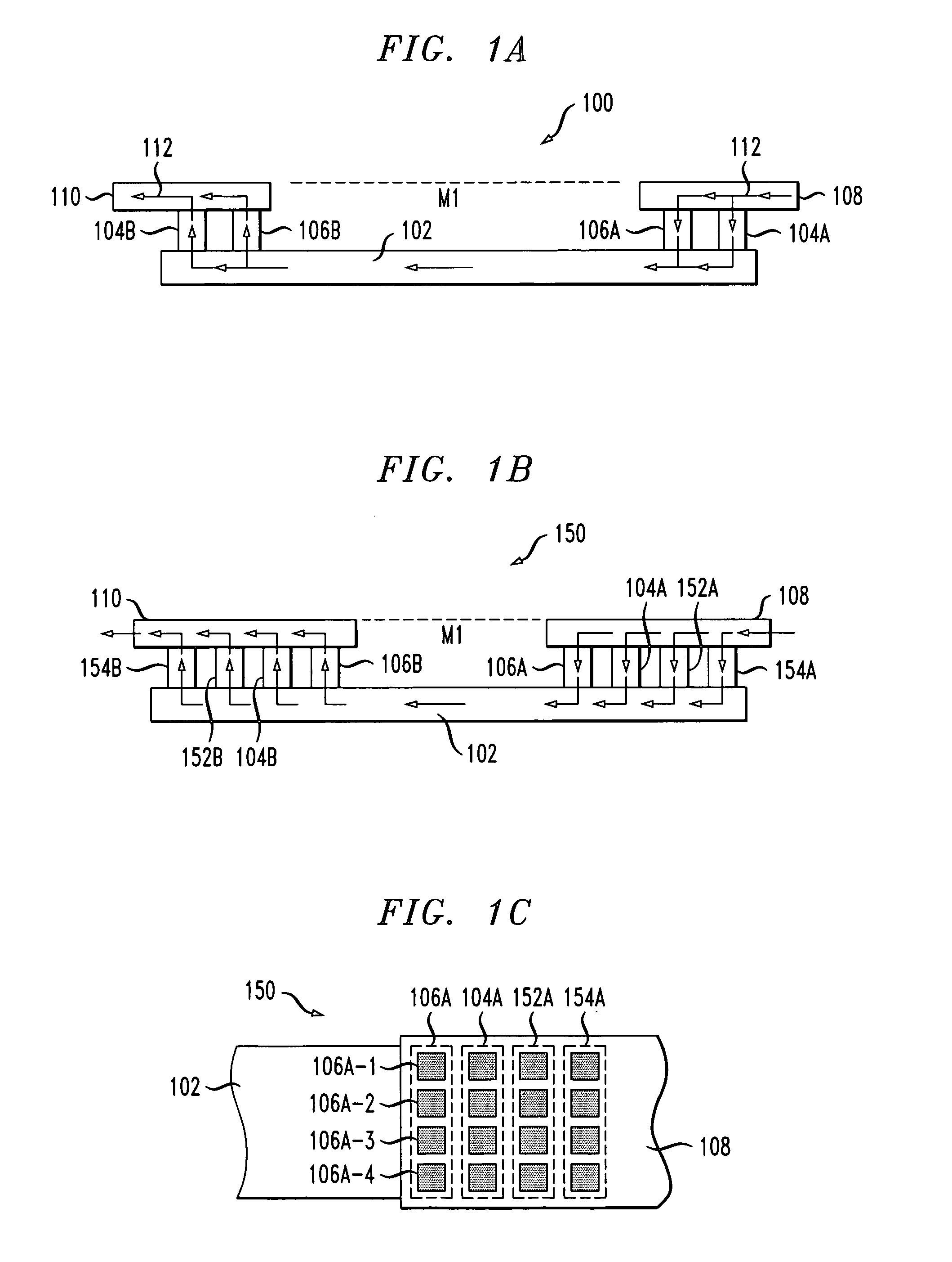
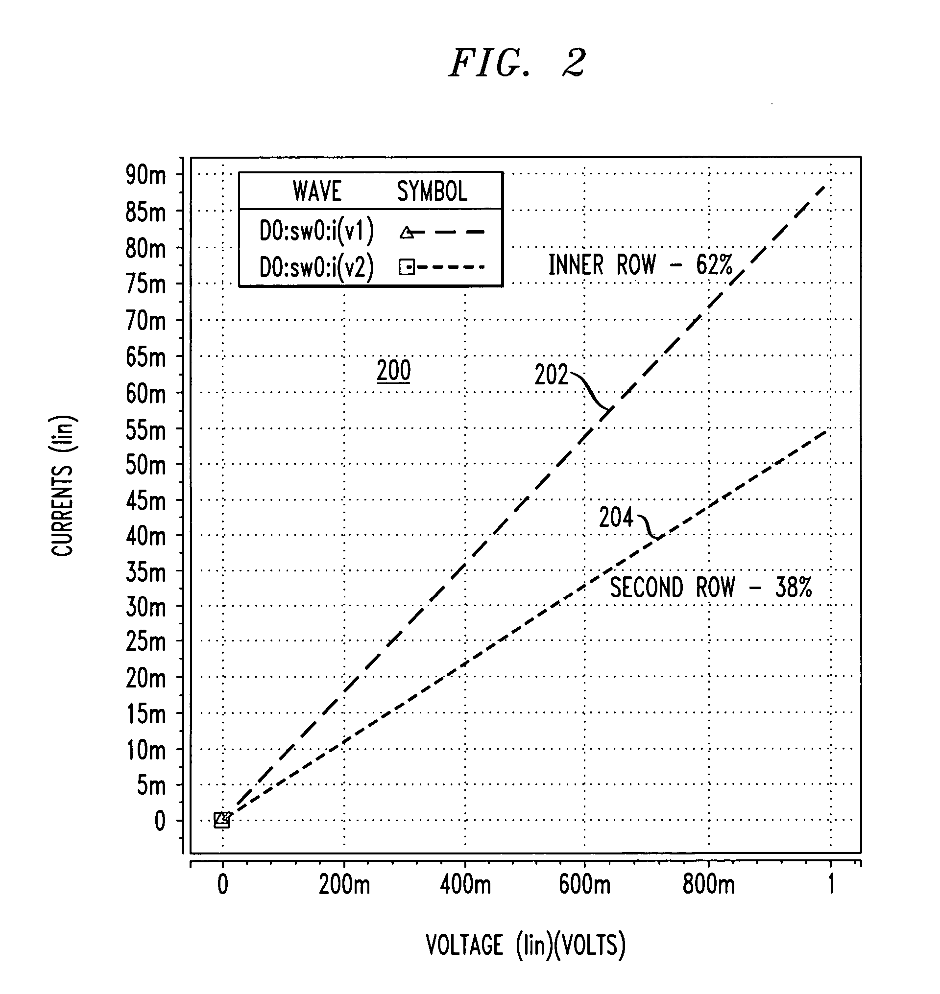
[0018]FIG. 1A depicts a cross section of an illustrative semiconductor resistor 100 which can be modified to implement the techniques of the present invention. The illustrative semiconductor resistor 100 includes a resistor body 102, a first conductive terminal 108 and a second conductive terminal 110. The first and second conductive terminals 108, 110 are electrically connected to the resistor body 102, at laterally opposite ends thereof, by two rows of contacts 104A, 106A and 104B, 106B, respectively....


PUM


Abstract

A semiconductor resistor comprises a resistor body formed on a semiconductor substrate and first and second conductive terminals electrically connected to the resistor body at opposite ends thereof. The semiconductor resistor further includes at least first and second conductive paths between at least one of the first and second conductive terminals and the resistor body. The at least one conductive terminal is configured such that a resistance of the at least one conductive terminal between the at least first and second conductive paths is substantially matched to a resistance of the resistor body between the at least first and second conductive paths. In this manner, a current distribution between the at least first and second conductive paths is substantially matched.

Description

FIELD OF THE INVENTION [0001] The present invention relates generally to semiconductor devices, and more particularly relates to techniques for forming a semiconductor resistor having improved reliability. BACKGROUND OF THE INVENTION [0002] A semiconductor resistor, as may be fabricated in an integrated circuit (IC) device, typically comprises a body portion formed of a material having a predetermined resistivity, often stated in units of ohms per square, associated therewith. Electrical connection to the body portion is generally provided by a plurality of metal contacts formed at opposite ends of the resistor body. The contacts at the ends of the resistor body may be connected to metal terminals for providing electrical interconnection with other components and / or structures in the IC device. [0003] Since the metal terminals connected to the contacts at each end of the semiconductor resistor are generally of significantly lower resistance in comparison to the resistance of the res...

Claims


Application Information

Patent Timeline
Patent Type & Authority Applications(United States)
IPC IPC(8): H01C1/14H01L21/02H01L23/522H01L27/08
CPCH01C1/14H01L28/20H01L27/0802H01L23/5228H01L2924/0002H01L2924/00
Inventor BHATTACHARYA, DIPANKARKRIZ, JOHN CHRISTOPHERSIEGEL, STEFAN ALLENSIMKO, JOSEPH E.SMOOHA, YEHUDA
Owner BELL SEMICON LLC
Why Eureka
Try Eureka