System and method for production testing of high speed communications receivers

a technology of communication receiver and production test, which is applied in the direction of electronic circuit testing, measurement devices, instruments, etc., can solve the problems of inability to support jitter tolerance testing using these methodologies, introduce errors and loss of synchronization, and limited circuit flexibility

Inactive Publication Date: 2005-08-04
MELLANOX TECHNOLOGIES LTD
View PDF5 Cites 117 Cited by
  • Summary
  • Abstract
  • Description
  • Claims
  • Application Information

AI Technical Summary

Benefits of technology

[0012] The present invention successfully provides a method and system for testing high-speed mu

Problems solved by technology

The flexibility of the circuit is limited due to its implementation as a BIST and as part of a semiconductor device.
Jitter is the perturbation of a signal in time or phase that can introduce errors and loss o

Method used


Image

  • System and method for production testing of high speed communications receivers
  • System and method for production testing of high speed communications receivers
  • System and method for production testing of high speed communications receivers

Examples


Embodiment Construction

[0018] The present invention is of a system and method for automatic production testing of jitter tolerance in multi-gigabit receivers using automatic test equipment. Specifically, the present invention can be used to perform simultaneous production testing of multiple serializer / deserializer ports on a semiconductor device.

[0019] The principles and operation of a system and method for automatic production testing of jitter tolerance in multi-gigabit receivers using automatic test equipment, according to the present invention, may be better understood with reference to the drawings and the accompanying description.

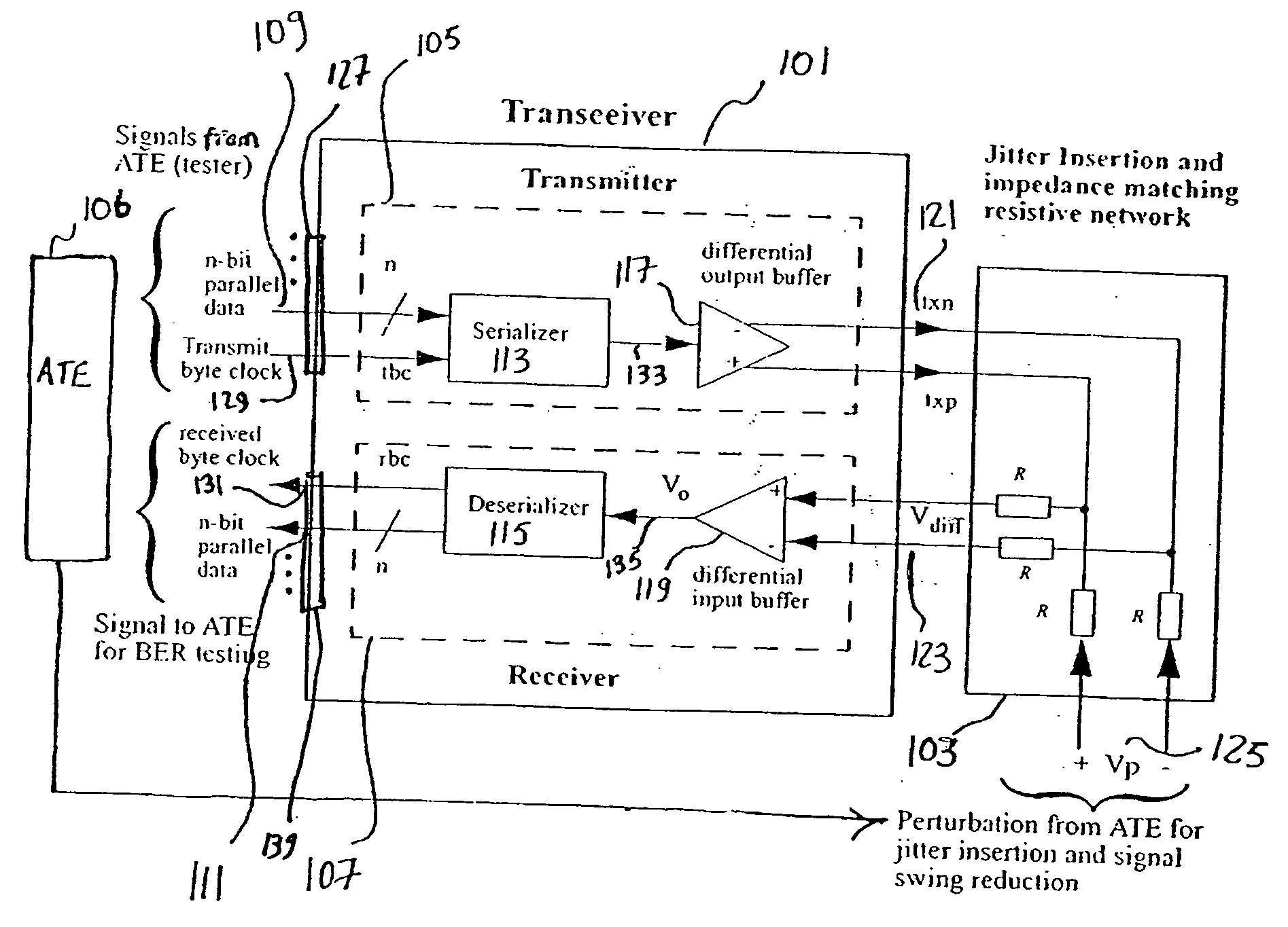
[0020] Referring now to the drawings, FIG. 1 illustrates jitter tolerance production testing, according to an embodiment of the present invention. A semiconductor device under test includes multiple transceivers 101. For simplicity, only one transceiver 101 is shown in FIG. 1. Transceiver 101 includes a transmitter 105 and a receiver 107. Parallel data of n bits 109 are ...


PUM


Abstract

A method for testing a semiconductor device with a multi-gigabit communications receiver includes combining a data output from a high-speed communications transmitter with a perturbation signal generated by automatic test equipment. The combined signal data signal including jitter and low voltage swings is input to the communications receiver port under test. The automatic test equipment determines the bit error rate of the parallel data output from the receiver port under test. This test method is appropriate for semiconductor devices with multiple transceiver ports.

Description

FIELD AND BACKGROUND OF THE INVENTION [0001] The present invention relates to production testing of high-speed communications receivers and, more particularly, to a system and method of inserting jitter into multi-gigabit per second receivers for production testing. [0002] Fast computer communications technologies have been emerging that utilize serial point-to-point physical links with data rates well beyond 1 Gigabit / sec (Gbps). These communications technologies, including Infiniband™ (2.5 Gbps), fiber channel (3.2 Gbps), SONET and Gigabit Ethernet, are being adopted in many applications including communications between servers, back-bone communications and data storage. High volume production has begun of new semiconductor devices that enable these technologies. Each of the new multi-gigabit semiconductor devices includes multiple (e.g 32 or 96) serializer / deserializer ports. As part of the production testing of these semiconductor devices, the multiple serializer / deserializer po...

Claims


Application Information

Patent Timeline
IPC IPC(8): G01R31/28G01R31/317
CPCG01R31/3171G01R31/2834
Inventor HULIEHEL, FAKHRALDEN A.
Owner MELLANOX TECHNOLOGIES LTD
Why Eureka
Try Eureka