
Error detection and correction scheme for a memory device

a memory device and error detection technology, applied in the field of memory devices, can solve the problems of slowness, inability to robustly solve errors, and inability to quickly solve errors,

Active Publication Date: 2005-08-04
MICRON TECH INC
View PDF16 Cites 226 Cited by
  • Summary
  • Abstract
  • Description
  • Claims
  • Application Information

AI Technical Summary

Benefits of technology

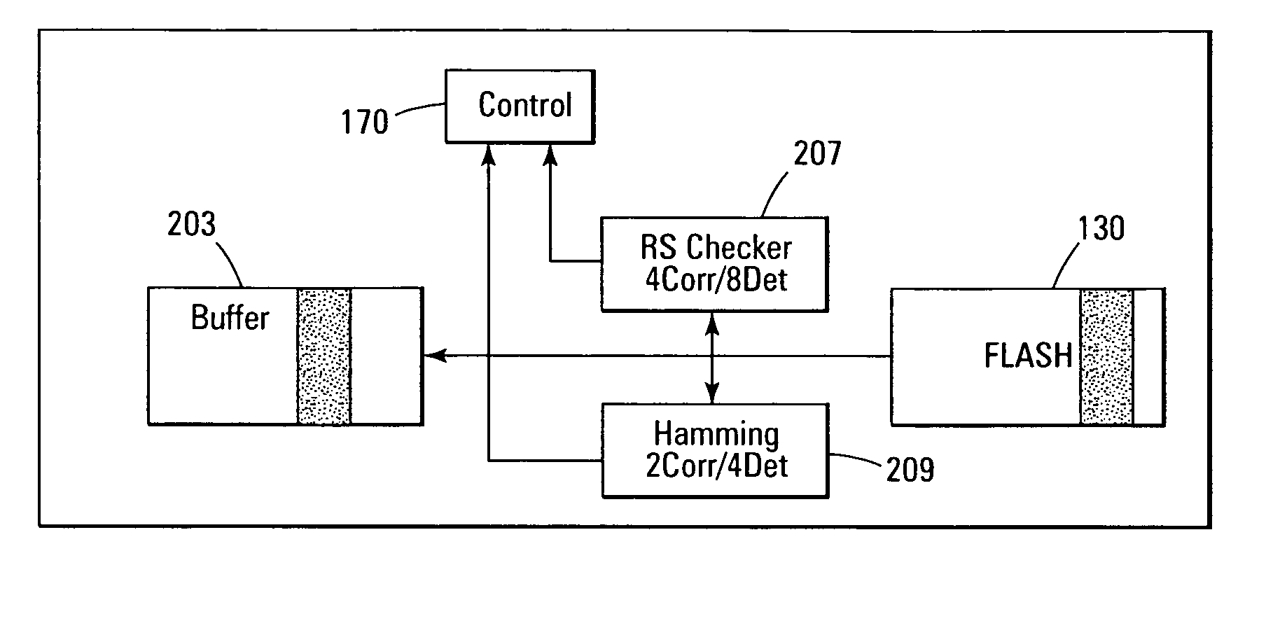
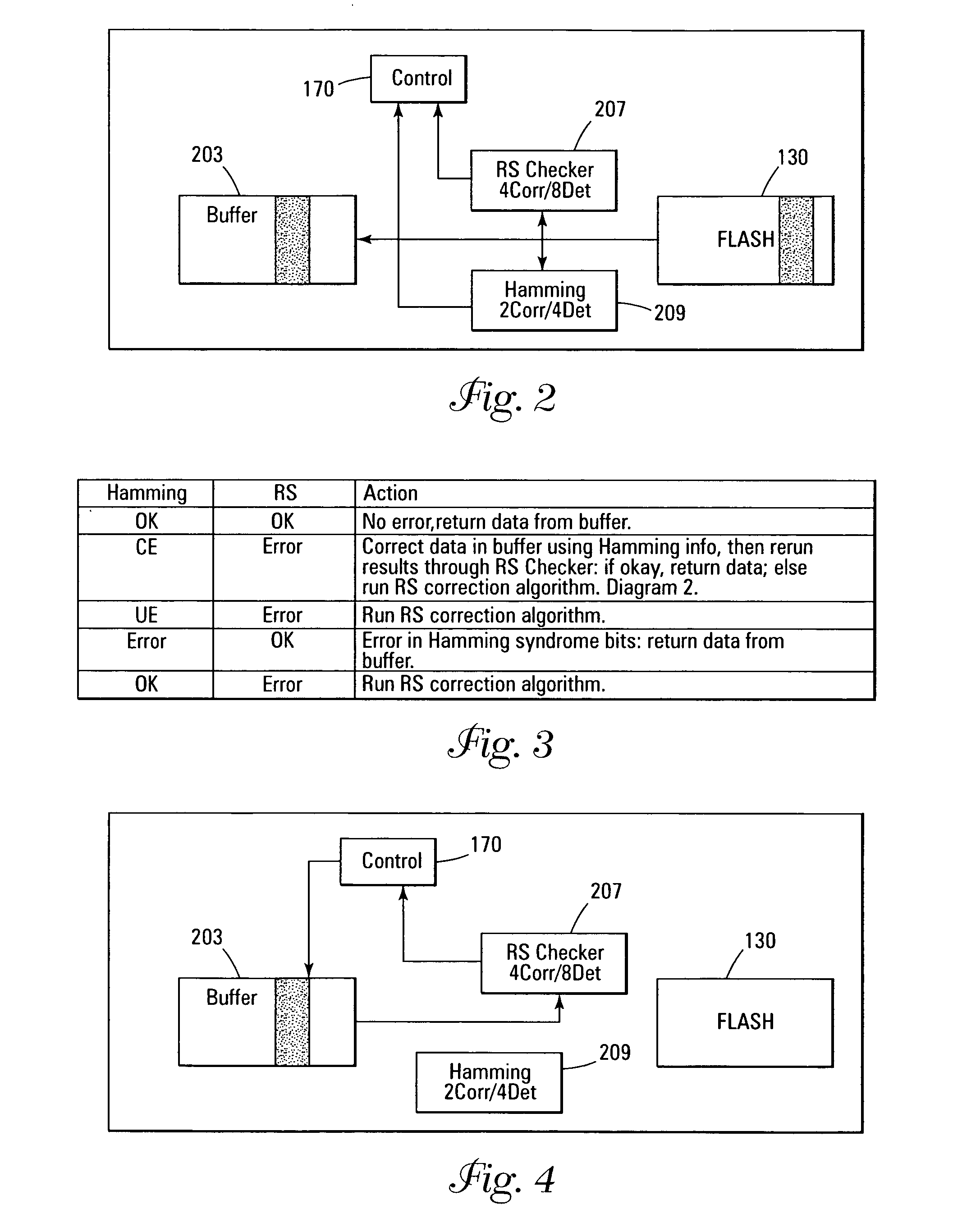
The present invention is a method for error detection and correction in a memory device. The method involves reading data from the memory array, performing two error detection operations in parallel, and reporting the results to the controller. The error corrected data is then stored in the data buffer. The first error detection operation is a Hamming code and the second error detection is a Reed-Solomon code. The technical effect of this invention is to improve the accuracy and reliability of memory devices by detecting and correcting errors in a timely manner.

Problems solved by technology

However, each of these schemes has drawbacks.
The Hamming code is faster than many error correction schemes but is not as robust.
The Reed-Solomon code is very robust but is relatively slow.

Method used


Image

  • Error detection and correction scheme for a memory device
  • Error detection and correction scheme for a memory device
  • Error detection and correction scheme for a memory device

Examples


Embodiment Construction

[0017] In the following detailed description of the invention, reference is made to the accompanying drawings that form a part hereof, and in which is shown, by way of illustration, specific embodiments in which the invention may be practiced. In the drawings, like numerals describe substantially similar components throughout the several views. These embodiments are described in sufficient detail to enable those skilled in the art to practice the invention. Other embodiments may be utilized and structural, logical, and electrical changes may be made without departing from the scope of the present invention. The following detailed description is, therefore, not to be taken in a limiting sense, and the scope of the present invention is defined only by the appended claims and equivalents thereof.

[0018] The following embodiments of the present invention are discussed with reference to a flash memory device, including both NAND and NOR-type flash devices. However, the present invention ...


PUM


Abstract

Data is read from a memory array. Before being stored in a data buffer, a Hamming code detection operation and a Reed-Solomon code detection operation are operated in parallel to determine if the data word has any errors. The results of the parallel detection operations are communicated to a controller circuit. If an error is present that can be corrected by the Hamming code correction operation, this is performed and the Reed-Solomon code detection operation is performed on the corrected word. If the error is uncorrectable by the Hamming code, the Reed-Solomon code correction operation is performed on the word.

Description

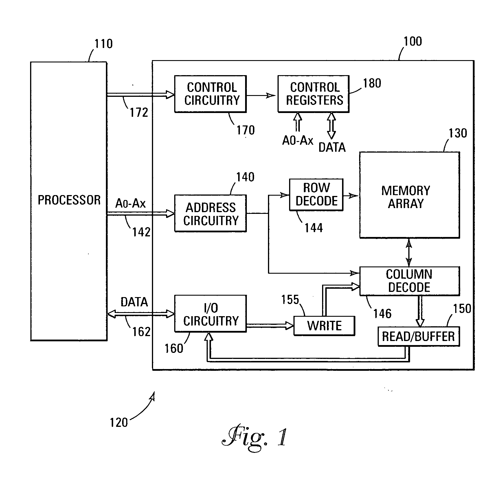
TECHNICAL FIELD OF THE INVENTION [0001] The present invention relates generally to memory devices and in particular the present invention relates to error correction in memory devices. BACKGROUND OF THE INVENTION [0002] Memory devices are typically provided as internal, semiconductor, integrated circuits in computers or other electronic devices. There are many different types of memory including random-access memory (RAM), read only memory (ROM), dynamic random access memory (DRAM), synchronous dynamic random access memory (SDRAM), and flash memory. [0003] A typical flash memory comprises a memory array, which includes a large number of memory cells. The flash memory is differentiated from other non-volatile memory in that flash memory cells can be erased and reprogrammed in blocks instead of one byte at a time. [0004] Flash memory devices typically have some type of error detection and correction that provides greater reliability. For example, if a design in which the memory device...

Claims


Application Information

Patent Timeline
Patent Type & Authority Applications(United States)
IPC IPC(8): G06F11/10H03M13/29
CPCH03M13/096G06F11/1008
Inventor RADKE, WILLIAM H.SWAMINATHAN, SHUBAKEAYS, BRADY L.
Owner MICRON TECH INC
Learn More