
Back contact and back reflector for thin film silicon solar cells

a back contact and solar cell technology, applied in the field of silicon solar cells, can solve the problems of reducing the performance of pv modules, reducing the reflectivity properties of metallic films, and affecting the performance of back contacts based on silver or aluminum

Inactive Publication Date: 2005-08-11
UNAXIS BALZERS LTD
View PDF0 Cites 82 Cited by
  • Summary
  • Abstract
  • Description
  • Claims
  • Application Information

AI Technical Summary

Problems solved by technology

First, the reflectivity and conductivity of metallic back contacts based on silver or aluminum are very sensitive to moisture and oxidation when used in photo voltaic (PV) modules over long-term outdoor applications.
If the PV modules are not properly sealed or if the seal breaks down over a period of time and becomes weak the sensitivity of the back contacts will degrade thus leading to a substantial decrease in the reflectivity properties of the metallic film and ultimately leading to a decrease in performance of the PV modules.
Second, the application of the metallic back reflector involves an additional production step thus requiring metal deposition equipment.
The regulation process is typically expensive which leads to increased production costs.
In order to reduce cost the regulation process may at times be omitted which leads to poor cell quality.
Another disadvantage is that it is difficult to provide a good adherence of the metallic back reflective layer to the cell, which leads to problems in long term evaluation of solar cells.
However, for microcrystalline silicon cells having a low absorption coefficient the light having a wavelength near the infrared region, e.g. over 1100 nm, cannot be absorbed by the silicon layer and thus the light would be lost without a back reflective layer.
However, the combination of such pigmented dielectric reflectors with TCO films has neither been described nor considered.

Method used


Image

  • Back contact and back reflector for thin film silicon solar cells
  • Back contact and back reflector for thin film silicon solar cells

Examples


Embodiment Construction

[0017] It should be noted that in the following description the term “reflective” or “reflector” is used in describing the white reflective media layer even though the white media according to the present invention does not necessarily act as a perfect specular reflector as does the metal reflective layer. However, the white reflective media re-scatters the light in many spatial directions from one incident beam. Thus it is better described as diffusive reflector.

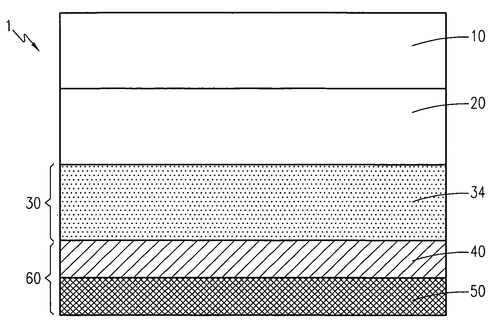
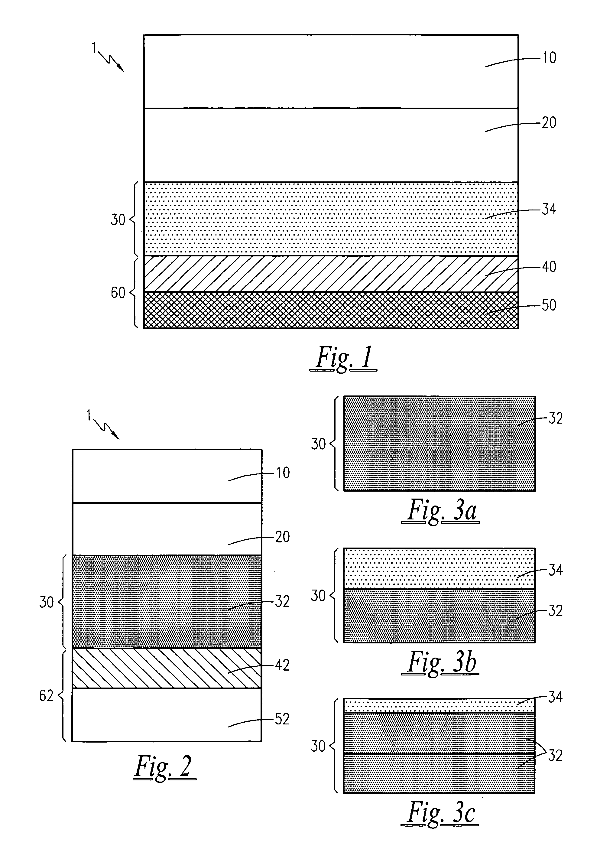
[0018] Referring now to the drawings, FIG. 2 shows a thin film silicon solar cell 1 according to the present invention that may be used in a wafer based silicon PV module. The cell 1 includes a carrier substrate layer 10, a front contact layer 20, a silicon solar cell layer 30, and a back contact 62 comprising a TCO contact layer 42 and a back reflective layer 52.

[0019] The substrate layer 10 and the front contact layer 20 are similar to the layers 10 and 20 shown in FIG. 1. More specifically, the substrate layer 10 is a ...


PUM


Abstract

A thin film silicon solar cell for use in photovoltaic cells having a carrier substrate, a front transparent conductive oxide contact, a thin film silicon solar cell layer having at least one layer of hydrogenated microcrystalline silicon or nanocrystalline silicon, and a back contact having a transparent conductive oxide contact layer and a back reflective layer comprising a white pigmented dielectric reflective media.

Description

[0001] This application claims the benefit of U.S. Provisional Patent Application Ser. No. 60 / 542,382 filed Feb. 6, 2004, the contents of which are incorporated herein by reference.FIELD OF THE INVENTION [0002] The present invention relates to silicon solar cells and more specifically the present invention is directed to improving the light trapping capability of thin film silicon solar cells. BACKGROUND OF THE INVENTION [0003] The light-trapping capability is related to the efficiency of thin film silicon solar cells. Improving the light-trapping capabilities of the silicon solar cell improves the cell efficiency and reduces the thickness of the cell, which improves the stability of thin film solar cells. Improving the light-trapping capability to produce a high quality light-trapping or light-confinement thin film silicon solar cell is attributed to the back contact. The back contact consists of two layers: 1) a highly textured transparent conductive oxide (TCO) front layer and 2)...

Claims


Application Information

Patent Timeline
IPC IPC(8): H01L31/052
CPCH01L31/056Y02E10/52Y02E10/548
Inventor MEIER, JOHANNESKROLL, ULRICHBUCHEL, ARTHUR
Owner UNAXIS BALZERS LTD
Learn More