Plasma etching chamber and plasma etching system using same

a plasma etching and plasma technology, applied in the direction of electrical equipment, basic electric elements, electric discharge tubes, etc., can solve the problems of difficult waste-disposing solution, affecting the plasma space, and affecting the etching effect of plasma etching, etc., to achieve the effect of limiting the plasma spa

Active Publication Date: 2005-08-11
SOSUL
View PDF5 Cites 97 Cited by
  • Summary
  • Abstract
  • Description
  • Claims
  • Application Information

AI Technical Summary

Benefits of technology

[0016] According to another aspect of the present invention, the etching chamber includes a stage mounted with a wafer, a ring-shaped top anode and a ring-shaped bottom cathode placed around the periphery of the wafer while facing each other and a view-ring placed at the outer circumference of the ring-shaped top anod

Problems solved by technology

For the fabrication of an integrated circuit, thin film process and dry etching process are very important but the film material is unnecessarily deposited at the periphery of the wafer during the thin film process, and in addition, with the dry cleaning of the top surface of the wafer through plasma etching, the by-product generated during the plasma etching is not completely exhausted, but deposited throughout the top, the lateral and the bottom sides of the periphery of the wafer as particles.
The periphery of the wafer is not used to form a semiconductor chip, but the film material and the particles left thereat (referred to hereinafter as the “particles”) cause serious damages to the semiconductor chips during the subsequent semiconductor processing steps.
The particl

Method used


Image

  • Plasma etching chamber and plasma etching system using same
  • Plasma etching chamber and plasma etching system using same
  • Plasma etching chamber and plasma etching system using same

Examples


Embodiment Construction

[0036] Preferred embodiments of the present invention will be now explained to make easy understanding of the advantages and the merits thereof.

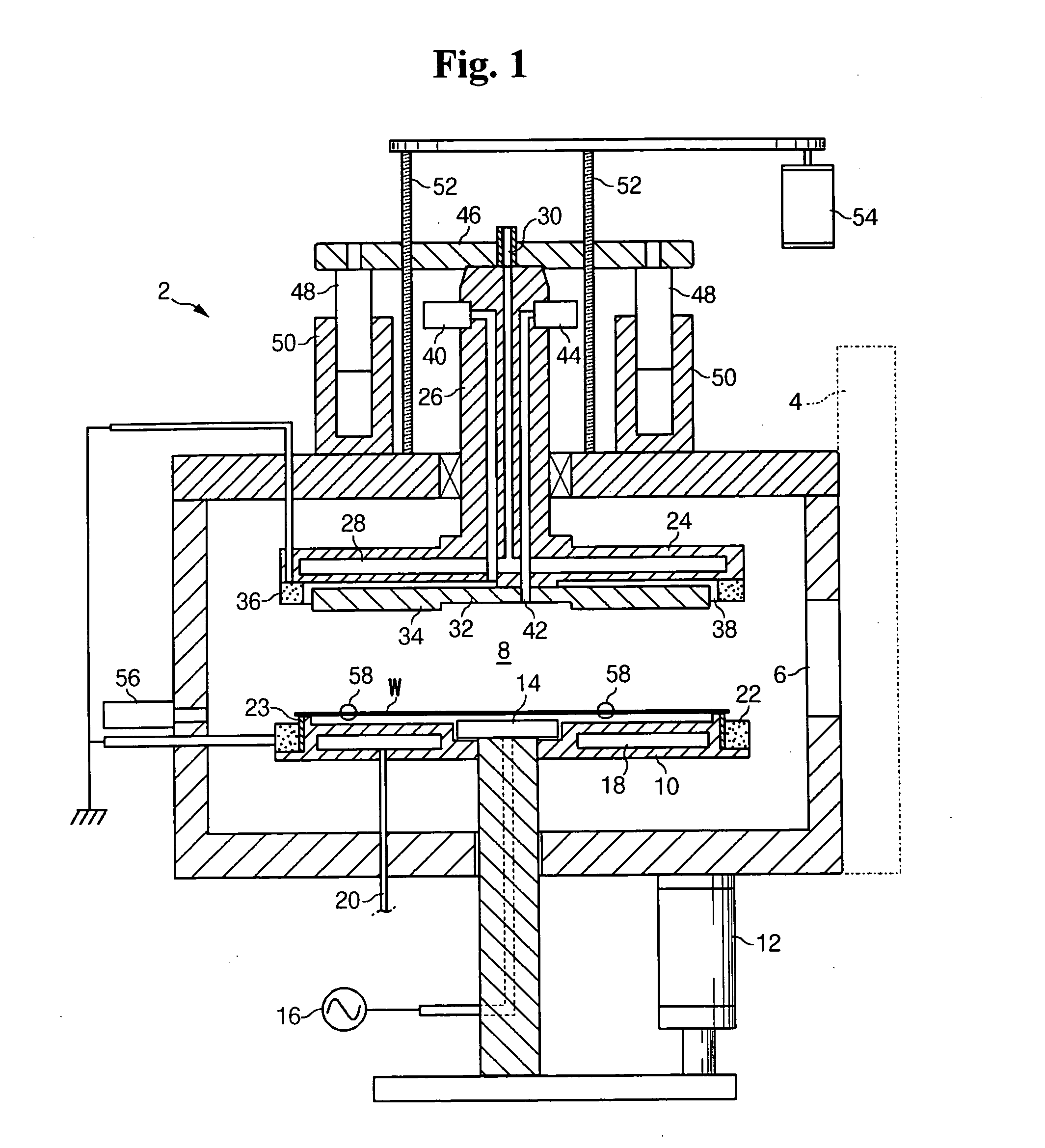
[0037]FIG. 1 illustrates the structure of an etching chamber according to an embodiment of the present invention.

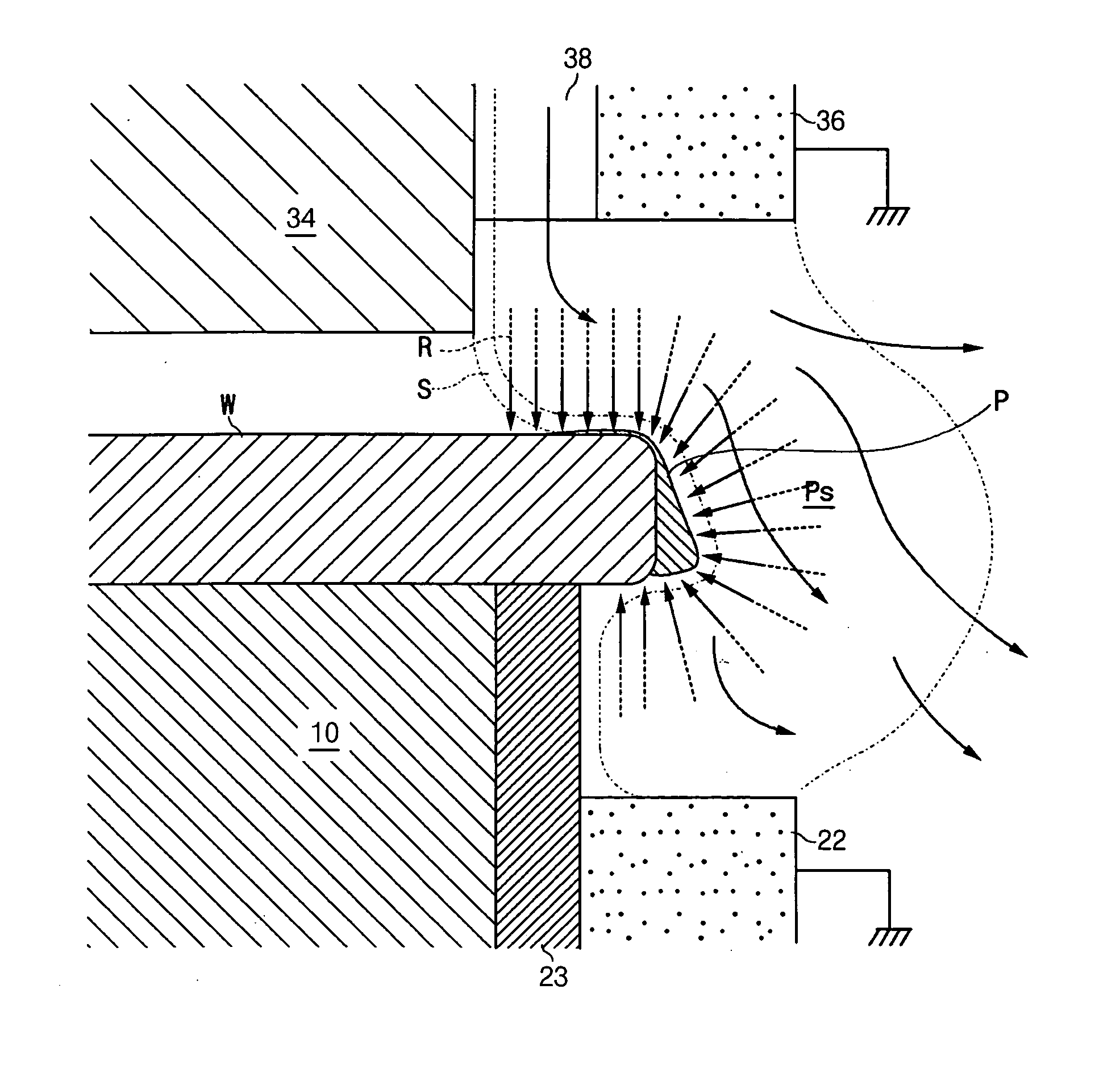
[0038] As shown in FIG. 1, the chamber 2 has an inner space 8 isolated from the outside by closing a door 4 of a gate 6 through which a wafer W goes in or out. A stage 10 is placed at the center of the inner space 8 to mount the wafer W thereon.

[0039] With the isolation of the inner space 8 from the outside, the atmosphere thereof is controlled to be under the low pressure of about 10−1-10−3 Torr.

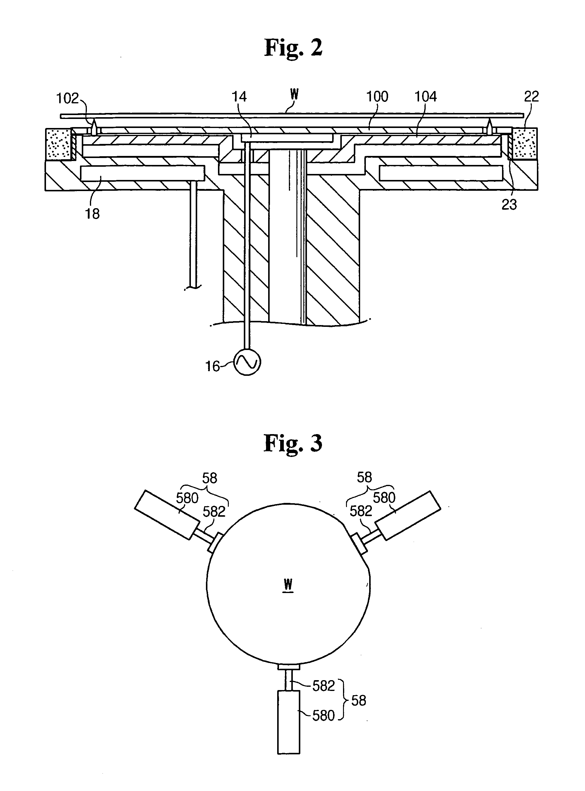
[0040] A cathode 14 is placed at the center of the top surface of the stage 10 such that it can be elevated by an actuator 12, and connected to a plasma oscillator 16. A water jacket 18 is provided within the stage 10 to forcefully cool it such that a coolant can be circulated via at least two paths 20 communicated with the outside. A...


PUM

PropertyMeasurementUnit
Thicknessaaaaaaaaaa
Depthaaaaaaaaaa
Lengthaaaaaaaaaa

Abstract

Disclosed is a plasma etching chamber for completely dry-cleaning a film material and particles deposited at the periphery of a wafer through plasma etching while generating plasma at the top to the bottom sides of the periphery of the wafer. A pair of top and bottom anodes facing each other is placed around the periphery of the wafer under the application of radio frequency through a cathode. Alternatively, a top cathode and a bottom anode are placed around the periphery of the wafer while facing each other and a view-ring shields the area of the cathode, the anode and the wafer from the outside. A plasma etching system includes a plurality of the above-structured etching chambers. A handler takes wafers from a plurality of cassette stands or load ports, and posture-corrects the orientation frat locations of the wafers by a wafer alignment unit. The wafers are charged into the plasma etching chambers directly or via load lock chambers. The handler takes the etched wafers from the chambers, and returns the wafers to the cassettes or the load ports directly or via the load lock chambers.

Description

BACKGROUND OF THE INVENTION [0001] (a) Field of the Invention [0002] The present invention relates to a system of removing a film material and particles left at the periphery of a semiconductor wafer, and in particular, to a plasma etching chamber capable of completely removing a film material and particles left and deposited at the periphery of the dry etched wafer during plasma etching, and a plasma etching system using the same. [0003] (b) Description of Related Art [0004] For the fabrication of an integrated circuit, thin film process and dry etching process are very important but the film material is unnecessarily deposited at the periphery of the wafer during the thin film process, and in addition, with the dry cleaning of the top surface of the wafer through plasma etching, the by-product generated during the plasma etching is not completely exhausted, but deposited throughout the top, the lateral and the bottom sides of the periphery of the wafer as particles. [0005] That is...

Claims


Application Information

Patent Timeline
IPC IPC(8): H01L21/3065C23F1/00H01J37/32H01L21/02
CPCH01J37/32091H01L21/02082H01J2237/334H01J37/32532H01L21/3065
Inventor LIM, DONG-SOO
Owner SOSUL
Why Eureka
Try Eureka