Current mode transmitter capable of cancel channel charge error

a current mode transmitter and channel charge technology, applied in the field of data communication, can solve the problems of transmission errors, increased power dissipation, complex structure of current mode transmitters, etc., and achieve the effects of improving the performance of current transmission, improving the cut-off delay, and rapid and correct current transmissions

Inactive Publication Date: 2005-08-11
SAMSUNG ELECTRONICS CO LTD
View PDF10 Cites 2 Cited by
  • Summary
  • Abstract
  • Description
  • Claims
  • Application Information

AI Technical Summary

Benefits of technology

[0016] It is a feature of an embodiment of the present invention to counteract and cancel transmission current errors caused by a change in channel charges, which occurs while a transistor switches between operation regions.
[0017] It is another feature of an embodiment of the present invention to improve cut-off delay is improved, thus enabling rapid and correct current transmissions.
[0018] It is yet another feature of an embodiment of the present invention to provide an additional circuit added to a conventional transmitter for improving performance thereof that is structurally simple and requires negligible additional area in the circuit layout.

Problems solved by technology

Thus, the structure of the current mode transmitter is complicated, and power dissipation is increased, since current is continuously supplied from the high power supply voltage Vcc, is sunk to the low power supply voltage GND or sinks irrespective of a state of the output signal Iout.
The variation of the voltage drop in the parasitic capacitor Cgs changes the amount of the current flowing through the MOS transistor M2 and finally causes transmission errors.
Referring to FIGS. 2 and 3, when the inverted input signal Vinb switches from a high state to a low state, a rise in the voltage of the node X lags, thus resulting in a cut-off delay of the MOS transistor M2.
The cut-off delay results in a delay in switching of the output current.
As a result, a duty ratio of a current signal to be transmitted is deteriorated.

Method used


Image

  • Current mode transmitter capable of cancel channel charge error
  • Current mode transmitter capable of cancel channel charge error
  • Current mode transmitter capable of cancel channel charge error

Examples


Embodiment Construction

[0030] Korean Patent Application No. 2004-07829, filed on Feb. 6, 2004, in the Korean Intellectual Property Office, entitled: “Current Mode Transmitter Capable of Canceling Channel Charge Error,” is incorporated by reference herein in its entirety.

[0031] The present invention will now be described more fully with reference to the accompanying drawings, in which exemplary embodiments of the invention are shown. The invention may, however, be embodied in different forms and should not be construed as limited to the embodiments set forth herein. Rather, these embodiments are provided so that this disclosure will be thorough and complete, and will fully convey the scope of the invention to those skilled in the art. The same reference numerals are used to denote the same elements throughout the drawings.

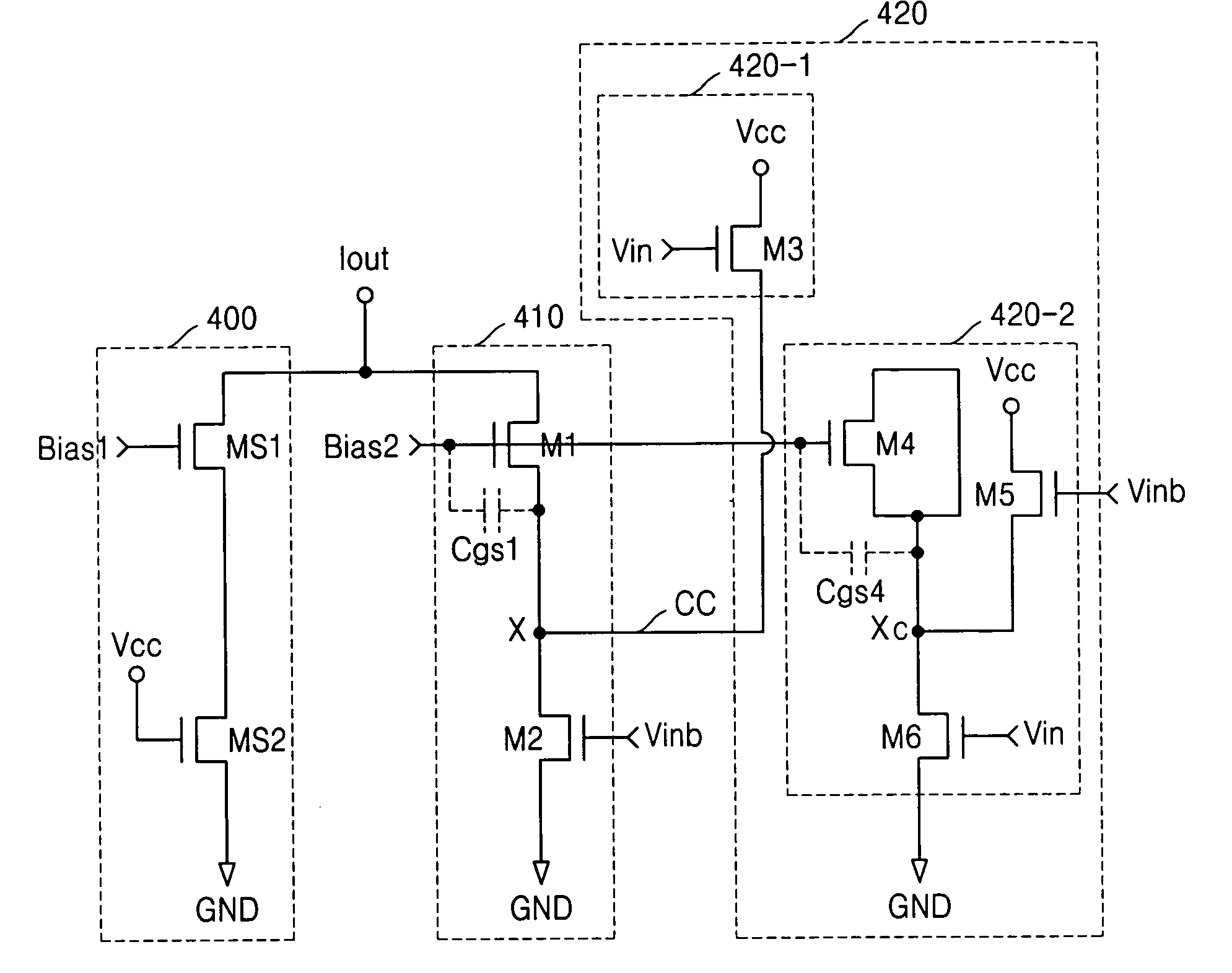
[0032]FIG. 4 is a circuit diagram of a current mode transmitter according to the present invention.

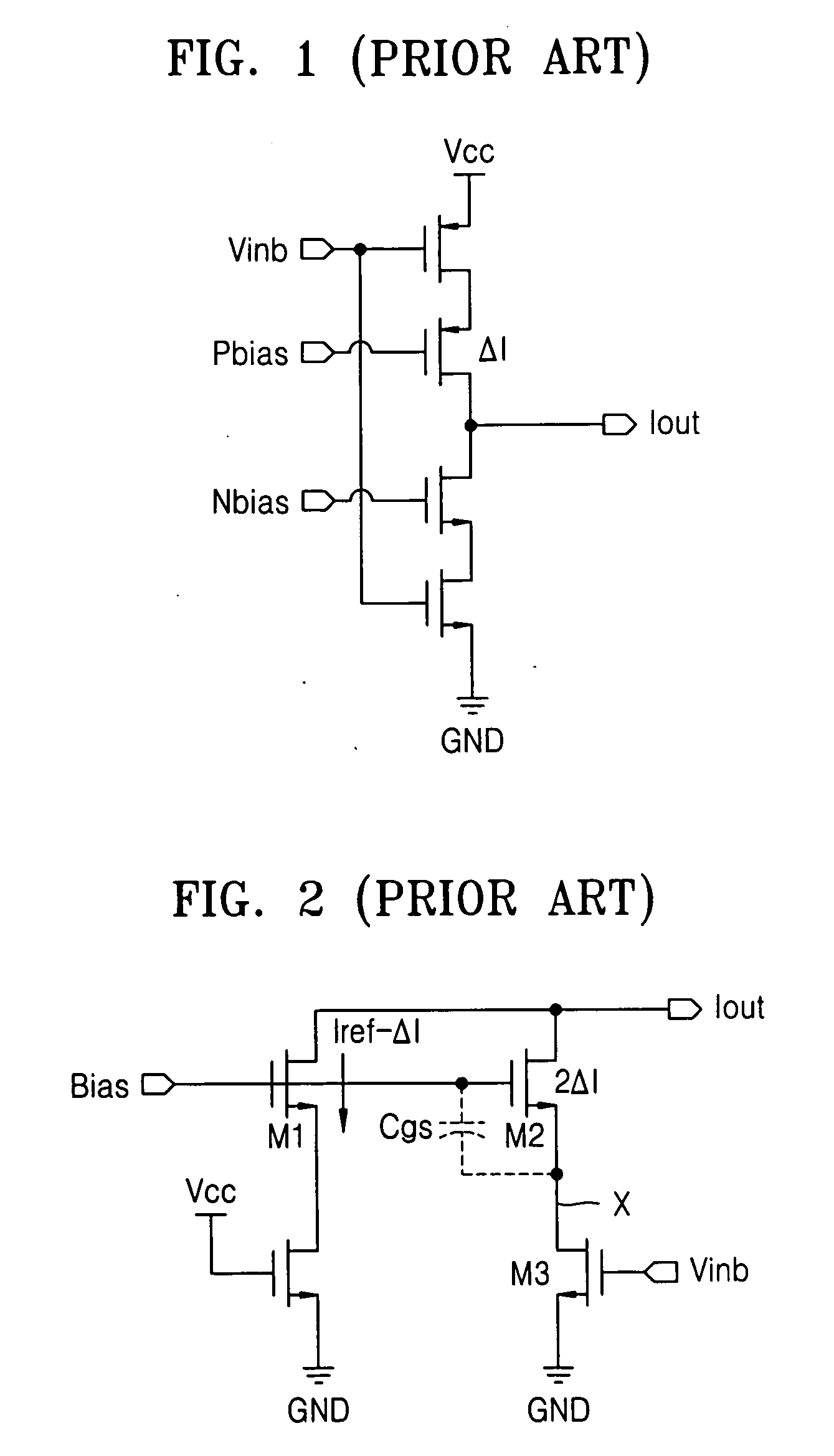
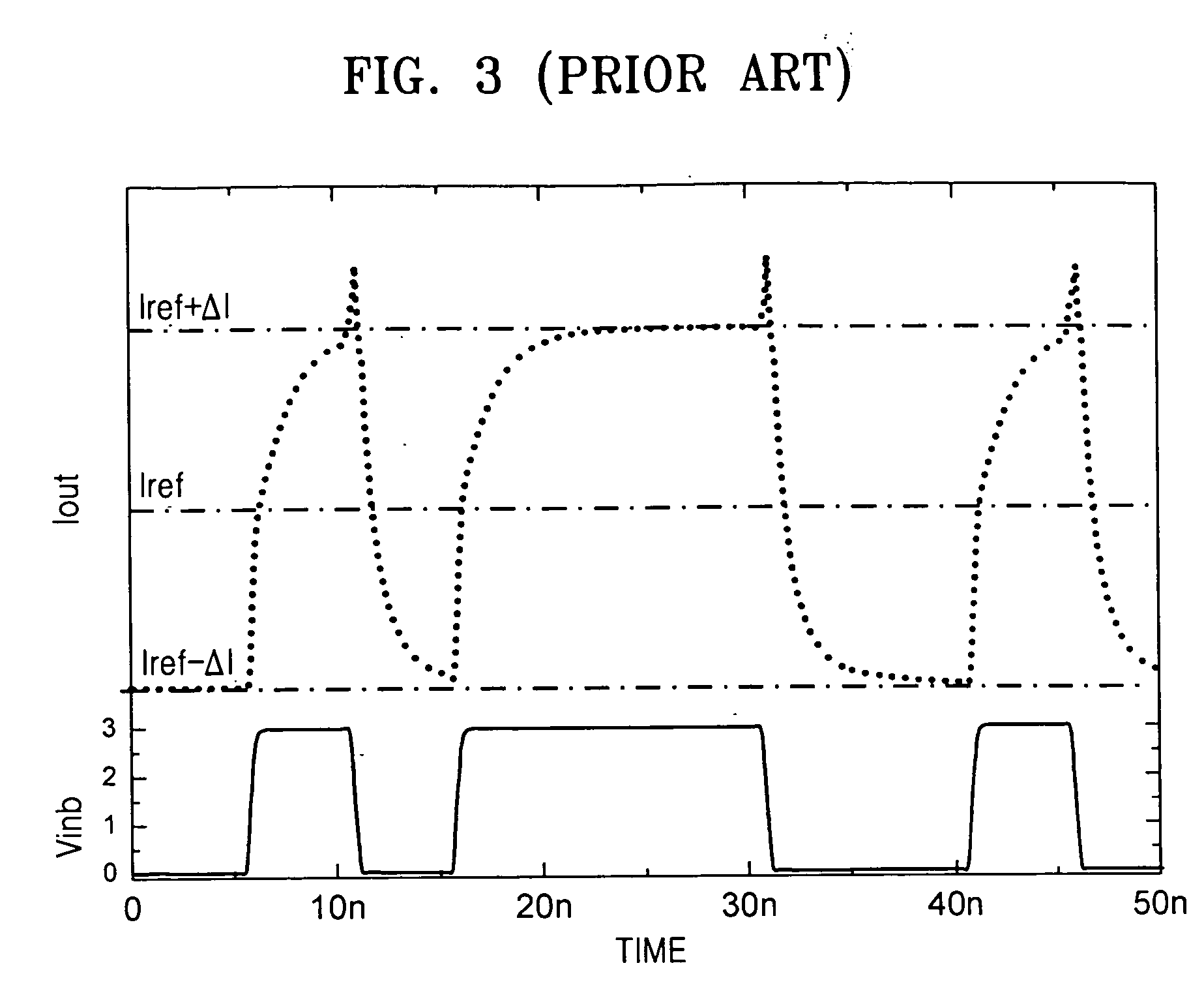
[0033] Referring to FIG. 4, the current mode transmitter includes a first sink curren...


PUM


Abstract

A current mode transmitter includes a first sink current path, through which a current flows from an output port according to a first bias voltage, a charge error canceller, which supplies a current from a high power supply voltage to a current control port in response to an input signal and counteracts a variation of a second bias voltage in response to an inverted input signal, which has an opposite polarity to that of the input signal, and the second bias voltage, and a second sink current path, which sinks current supplied from the output port in response to the second bias voltage and the inverted input signal, the second sink current path being controlled by the current control port. The input signal and the inverted input signal are complementary.

Description

BACKGROUND OF THE INVENTION [0001] 1. Field of the Invention [0002] The present invention relates to data communications. More particularly, the present invention relates to data communications using current signals. [0003] 2. Description of the Related Art [0004]FIG. 1 is a circuit diagram of a conventional current mode transmitter. [0005] Referring to FIG. 1, the current mode transmitter determines a logic state of an output signal Iout according to the voltage of the output signal Iout, which varies between a high power supply voltage Vcc and a low power supply voltage GND. To embody the current mode transmitter, a circuit for generating two bias voltages Pbias and Nbias is additionally required to supply the voltages to the current mode transmitter. Thus, the structure of the current mode transmitter is complicated, and power dissipation is increased, since current is continuously supplied from the high power supply voltage Vcc, is sunk to the low power supply voltage GND or sin...

Claims


Application Information

Patent Timeline
Patent Type & Authority Applications(United States)
IPC IPC(8): H04L25/02H03K19/017H03K19/0185H04L27/00
CPCH03K19/018521H03K19/01707H04L27/00
Inventor CHANG, IL-KWONJEON, YONG-WEON
Owner SAMSUNG ELECTRONICS CO LTD
Why Eureka
Try Eureka