Micro-lens array substrate and production method therefor, and projection type liquid crystal display unit using those

a technology of micro-lens array and production method, which is applied in the direction of photomechanical equipment, instruments, originals for photomechanical treatment, etc., can solve the problems of reducing the cost and size of the liquid crystal display device of the three-dimensional, the optical system is more complicated with a larger number of components, and the use of only 13 incident light, etc., to achieve high-quality micro-lens array substrate and low cost

Inactive Publication Date: 2005-08-11
SHARP KK
View PDF2 Cites 44 Cited by
  • Summary
  • Abstract
  • Description
  • Claims
  • Application Information

AI Technical Summary

Benefits of technology

[0019] Thus, since the present invention prevents a lens-pitch misregistration and does not require alignment of optical-axes for the micro-lens arrays, it becomes possible to produce a highly accurate micro-lens array substrate at low cost.

Problems solved by technology

However, it is difficult to reduce the cost and size of a liquid crystal display device of the three-panel mode, as it requires the color separation function and the image formation function, which consequently makes its optical system to become more complicated with a larger number of components.
However, a disadvantage of the liquid crystal display device of the single-panel mode is that it can use only a ⅓ of incident light due to absorption or reflection of light that occurs at its color filter.
This, however, poses the problem of high manufacturing cost associated with difficulties in optical-axes alignment, as described below.
This has made the production of double-layer micro-lens array substrates extremely difficult.
Moreover, a middle layer between the two layers of micro-lens array is another cause of difficulty in the optical-axes alignment.
However, in this case, the alignment mark observation systems still require accurate optical-axes alignment.
Thus, as described above, a middle layer between the two layers of micro-lens array has also been a cause of high cost of a positioning apparatus.

Method used


Image

  • Micro-lens array substrate and production method therefor, and projection type liquid crystal display unit using those
  • Micro-lens array substrate and production method therefor, and projection type liquid crystal display unit using those
  • Micro-lens array substrate and production method therefor, and projection type liquid crystal display unit using those

Examples


Embodiment Construction

[0038] An embodiment in accordance with the present invention is described below with references to the attached drawings.

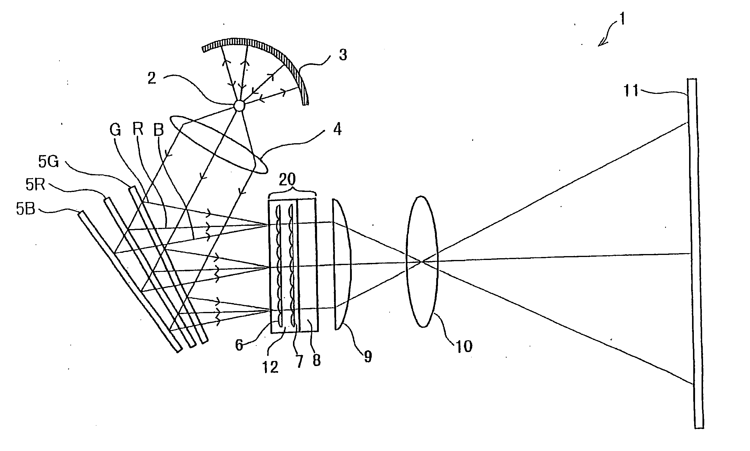
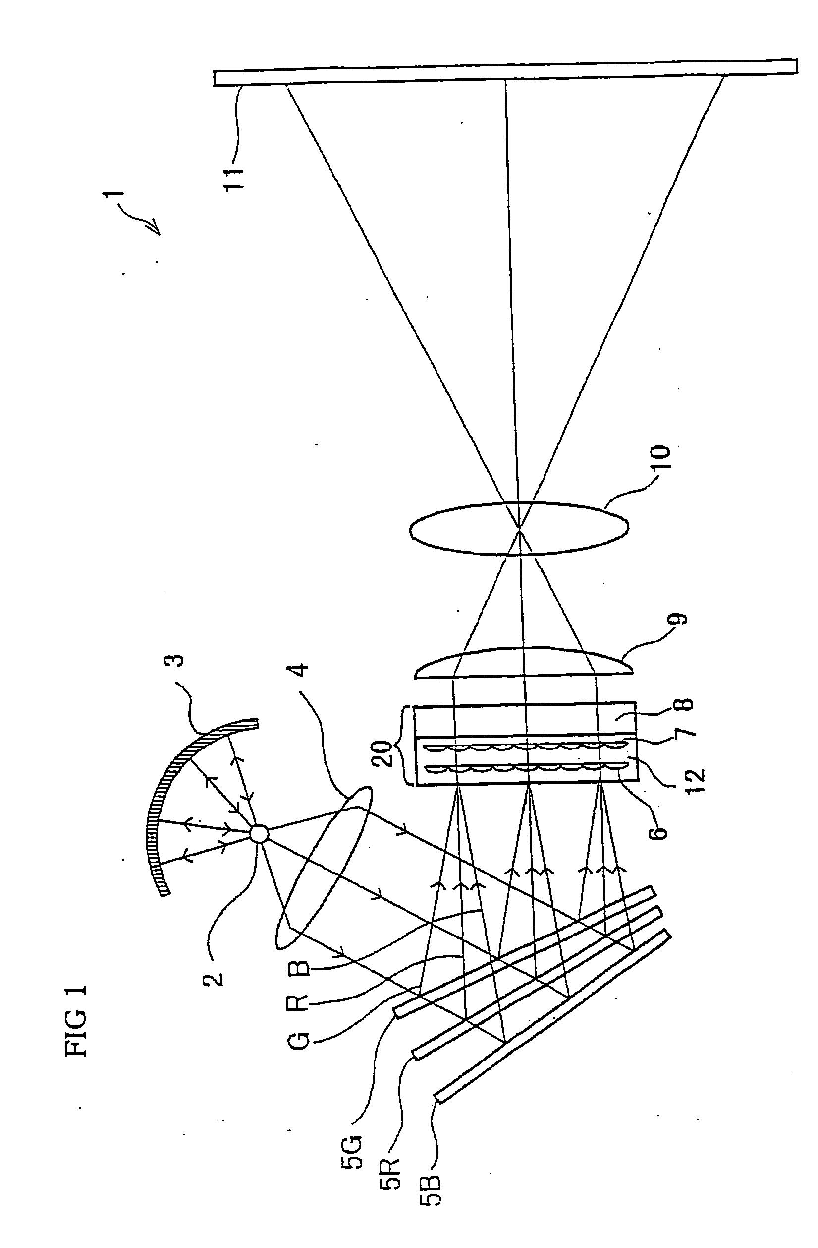
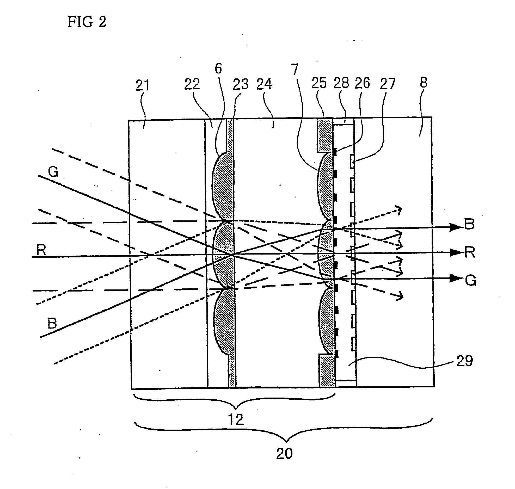
[0039]FIG. 1 is a cross sectional view showing the overall configuration of a projection type liquid crystal display device in accordance with the present invention, and FIG. 2 is a cross sectional view of a micro-lens array substrate and a liquid crystal display element in accordance with the present invention, used in a transmissive liquid crystal display device.

[0040] A projection liquid crystal display device 1 shown in FIG. 1 includes a spherical mirror 3 provided behind a white beam source 2. The spherical mirror 3 is positioned so that its center coincides with the emission center of light in the white beam source 2. In front of the white beam source 2, a condenser lens 4 is provided. The condenser lens 4 is positioned so that its focal point coincides with the emission center of light in the white beam source 2.

[0041] By such arrangement, a substantial...


PUM

PropertyMeasurementUnit
incident angleaaaaaaaaaa
thicknessaaaaaaaaaa
wavelengthaaaaaaaaaa

Abstract

In a micro-lens array substrate (12) that includes first and second micro-lens arrays (6, 7) respectively having a plurality of lenses, the first micro-lens array (6) is sandwiched between two inorganic dielectric substrates (21, 24), and the second micro-lens array (7) is formed on one of the two inorganic dielectric substrates (21, 24).

Description

TECHNICAL FIELD [0001] The present invention relates to a double-layered micro-lens array substrate, and a production method of the micro-lens array substrate. The invention also relates to a single-plate projection type liquid crystal display device using such a micro-lens array substrate for a liquid crystal display element. BACKGROUND ART [0002] Comparing with a projection cathode-ray tube display device, a projection type liquid crystal display device has more attractive features such as a wider range of color reproduction, better mobility due to small size and light weight, no need for a convergence adjustment as it is not affected by earth magnetism, and so on. Since the screen size of the projection type liquid crystal display device can be increased easily, the projection type liquid crystal display device is expected to prevail as a mainstream of home-use image display device in the future. [0003] Among color projection type image display modes utilizing liquid crystal disp...

Claims


Application Information

Patent Timeline
Patent Type & Authority Applications(United States)
IPC IPC(8): G02B3/00G02F1/13G02F1/1335G02F1/13357G03F7/20
CPCG02B3/0012G02B3/0056H04N9/3108G02F1/133526G02F1/133621G02B3/0068G02F1/1335
Inventor OKADA, KUNIAKINAGASAKA, YUKIKOKITAMURA, KAZUYASEKIMOTO, YOSHIHIROKURATA, YUKIONAKANISHI, HIROSHI
Owner SHARP KK
Why Eureka
Try Eureka