Dielectric multi layer thin film optical filter having predetermined wavelength optical characteristics, a method of manufacturing the same, a program for designing the same, and an optical add-drop system using the dielectric multi layer thin film optical filter

a optical filter technology, applied in the field of dielectric can solve the problems of difficult to apply existing optimization algorithms and difficult to design the film thickness of multi-layer thin film optical filter

Inactive Publication Date: 2005-08-11
FURUKAWA ELECTRIC CO LTD
View PDF5 Cites 31 Cited by
  • Summary
  • Abstract
  • Description
  • Claims
  • Application Information

AI Technical Summary

Problems solved by technology

However, as described above, in the case of a multi layer thin film optical filter such as a band-pass filter that allows an optical film thickness of only an integer times one-quarter of center wavelength λ (λ / 4) of a target band, it is difficult to apply existing optimization algorithm, and it is thus difficult to design a film thickness of the multi layer thin film optical filter as described above using the commercially available optical film structure designing software.

Method used


Image

  • Dielectric multi layer thin film optical filter having predetermined wavelength optical characteristics, a method of manufacturing the same, a program for designing the same, and an optical add-drop system using the dielectric multi layer thin film optical filter
  • Dielectric multi layer thin film optical filter having predetermined wavelength optical characteristics, a method of manufacturing the same, a program for designing the same, and an optical add-drop system using the dielectric multi layer thin film optical filter
  • Dielectric multi layer thin film optical filter having predetermined wavelength optical characteristics, a method of manufacturing the same, a program for designing the same, and an optical add-drop system using the dielectric multi layer thin film optical filter

Examples


example) 1

EXAMPLE (Design Example) 1

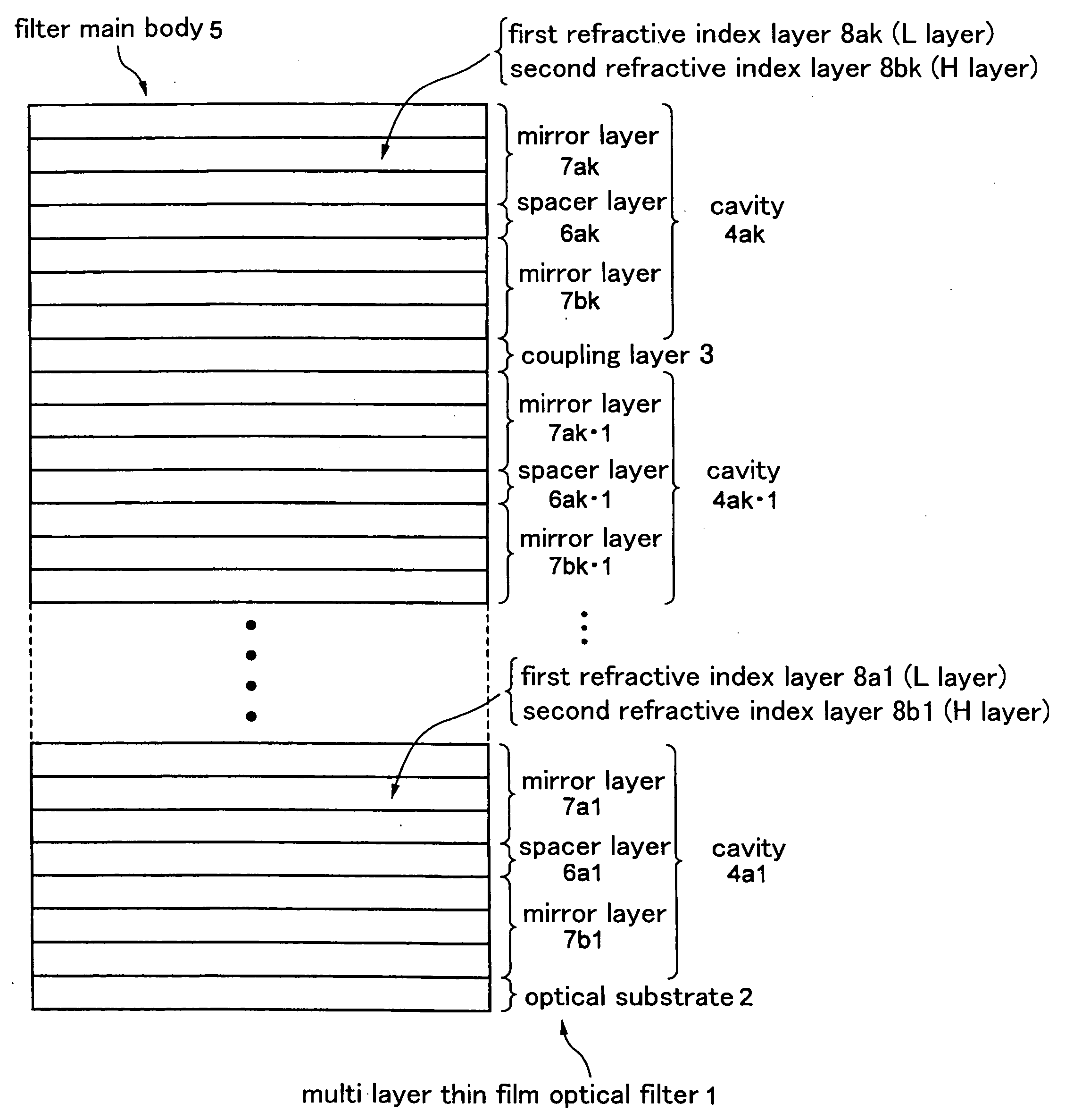
[0111] A multi layer thin film optical filter 1a was actually designed (see following expression (5)) using as the optical substrate 2 a substrate with a refractive index of 1.52 in a wavelength of 1550.0 nm, and the filter designing apparatus 10 (film structure designing scheme (algorithm)) of this embodiment while setting the center wavelength λ0 at 1555.0 nm. FIG. 5 shows wavelength dependence (transmittance wavelength characteristics) of transmittance E1 and equivalent admittance A1 that are optical characteristic values of the designed multi layer thin film optical filter 1a.

Air / L′H′L222−2142−2142−2202−2162−2202−2142−2142−222L / Sub   (5)

[0112] In addition, L′ and H′ represent reflection prevention layers (AR layers) with optical film thicknesses except λ0 / 4, and Sub represents the substrate 2.

[0113] As shown in FIG. 5, the multi layer thin film optical filter 1a designed by the film thickness designing scheme of this embodiment has optical characteri...

second embodiment

[0120] This embodiment describes designing a film structure of, for example, a 100 G-4skip0 band separator as the multi layer thin film optical filter 1c described in the first embodiment, using a designing scheme different from the designing scheme described in the first embodiment.

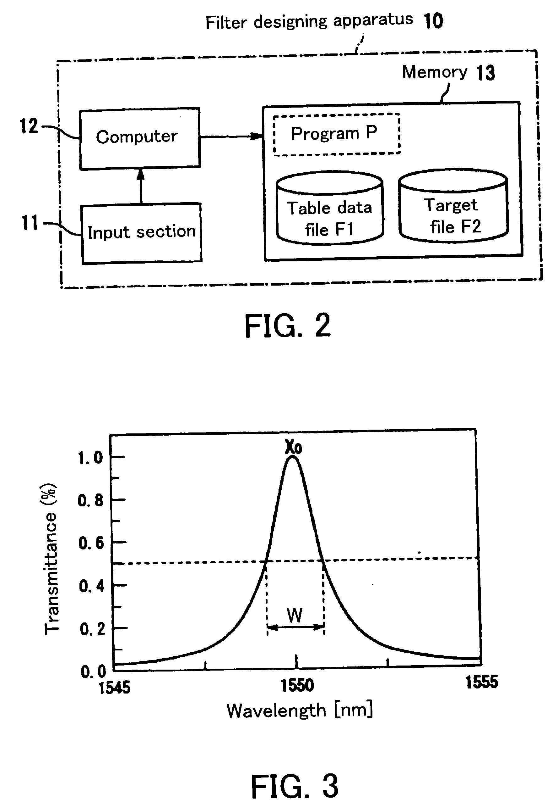
[0121] In other words, as illustrated in FIG. 7, a filter designing apparatus 30 is a computer system and provided with an input section 31 for a designer to operate and input information, a computer 32 connected to the input section 31, and a memory 33 as a storage medium which is connected to the computer 32 and beforehand stores a program P1 to execute filter designing processing as described later. In addition, as the storage medium, various storage media are applicable such as a semiconductor memory and magnetic memory.

[0122] In this embodiment, the program P1 stored in the memory 33 is different from the program P stored in the memory 13 in the filter designing apparatus 10 as illustrated in FIG....


PUM

PropertyMeasurementUnit
transmittanceaaaaaaaaaa
cutoff widthaaaaaaaaaa

Abstract

A dielectric multi layer thin film type band-pass filter provided with the function of transmitting a predetermined wavelength band, the function of reflecting a predetermined wavelength band or both functions, where a film structure of the dielectric multi layer thin film optical filter is configured of, with respect to the center wavelength λ as a reference of the optical film thickness, (1) mirror layers each comprised of alternately layered layers (H) of high refractive index material and layers (L) of low refractive index material each with an optical film thickness of λ/4, and (2) spacer layers each of which is configured in a combination of a layer (nH: n is an integer) of high refractive index material and a layer (nL: n is an integer) of low refractive index material each with an optical film thickness of λ/4 and has a total optical film thickness of an integral multiple of λ/2.

Description

FIELD OF THE INVENTION [0001] The present invention relates to a dielectric multi layer thin film optical filter, a method of manufacturing the same, a program for designing the same, and an optical add-drop system using the dielectric multi layer thin film optical filter. RELATED ART [0002] With the advent of the broadband era, great expectations are placed on a WDM (Wavelength Division Multiplexing) communication system (hereinafter, abbreviated as “WDM”) that multiplexes a plurality of optical signals with different wavelengths to transmit. [0003] One of key devices in the WDM communication system is a band-pass filter that selects a signal with a predetermined wavelength from the multiplexed optical signal and passes the selected signal through the filter. [0004] Used as the band-pass filter is a dielectric multi layer thin film optical filter (hereinafter, also referred to as simply “multi layer thin film optical filter) having a film structure (multi-cavity structure) where a ...

Claims


Application Information

Patent Timeline
Patent Type & Authority Applications(United States)
IPC IPC(8): G02B1/11G02B5/08G02B5/28G02B6/293G02B7/182G02B27/00
CPCG02B27/0012G02B5/281
Inventor ITO, TAKAHIROMINAGAWA, KAZUHIRO
Owner FURUKAWA ELECTRIC CO LTD
Why Eureka
Try Eureka