Multilayer pinned reference layer for a magnetic storage device

Active Publication Date: 2005-08-11
SAMSUNG ELECTRONICS CO LTD
View PDF7 Cites 13 Cited by
  • Summary
  • Abstract
  • Description
  • Claims
  • Application Information

AI Technical Summary

Benefits of technology

[0025] Further, according to an embodiment thereof, the invention may provide a magnetic memory device including: at least one ferromagnetic data layer characterized by an alterable orientation of magnetization; an intermediate layer in contact with the data layer; a multilayer pinned ferromagnetic reference layer in contact with the intermediate layer, opposite the data layer, the reference layer characterize

Problems solved by technology

Such manufacturing stresses may inadvertently weaken the reference layer 103, leading to an unstable reference field.
In addition, the characteristics of the data layer 101 may be unknowingly affected by heat during some manufacturing processes.
This type of structure is difficult to fabricate as the application of the intermediate layer 105 acting as the tunnel junction barrier effectively terminates the propagation of the crystal structure and reapplication of a new non-ferromagnetic seed layer is not possible as the spin dependence is then lost.
In addition, since the AFM layer does not have good texture, the resulting

Method used


Image

  • Multilayer pinned reference layer for a magnetic storage device
  • Multilayer pinned reference layer for a magnetic storage device
  • Multilayer pinned reference layer for a magnetic storage device

Examples


Example

[0034] Before proceeding with the detailed description, it is to be appreciated that the present invention is not limited to use or application with a specific type of magnetic memory. Thus, although the present invention is, for the convenience of explanation, depicted and described with respect to typical exemplary embodiments, it will be appreciated that this invention may be applied with other types of magnetic memory, any magnetic sensors or other magnetic field devices.

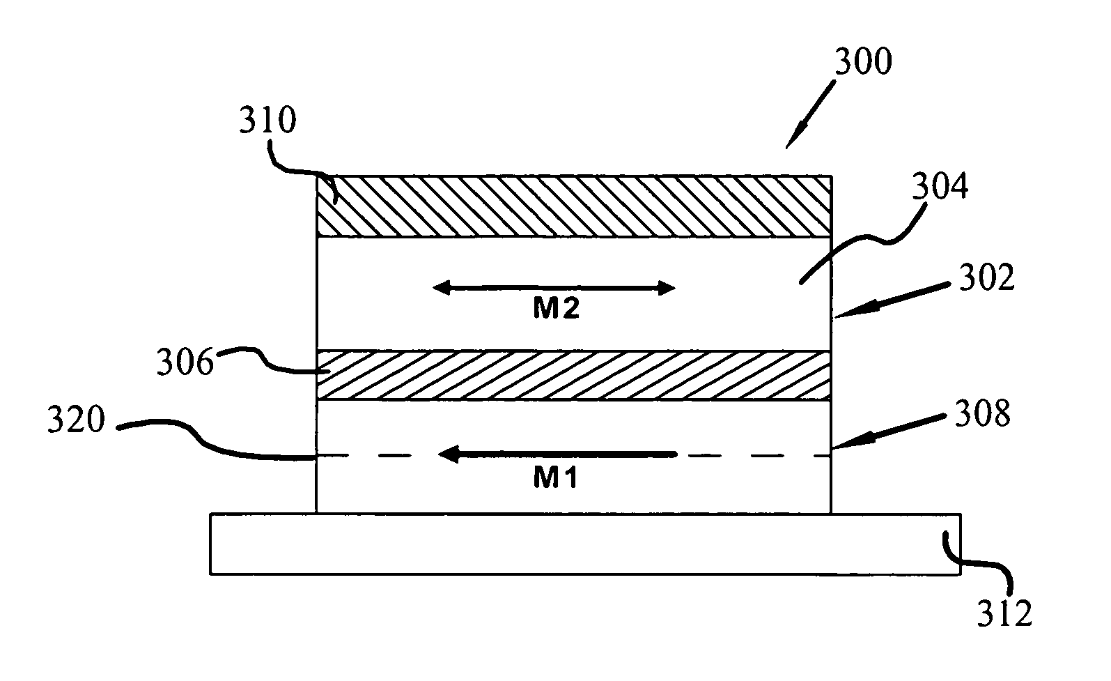
[0035] Referring now to the drawings, and more particularly to FIGS. 3A and 3B, there is shown a portion of a magnetic memory 300 comprising at least one spin valve memory cell 302 (SVM), according to an embodiment of the present invention. More specifically, SVM 302 has at least one ferromagnetic data layer 304, an intermediate layer 306, and a multilayer ferromagnetic pinned reference layer 308 (multilayer PRL). FIG. 3A conceptually illustrates a bottom-pinned spin valve structured device, while FIG. 3B illus...


PUM


Abstract

This invention provides a multilayer pinned reference layer for a magnetic device. In a particular embodiment a magnetic tunnel junction cell is provided. Each magnetic memory tunnel junction cell provides at least one ferromagnetic data or sense layer, an intermediate layer in contact with the data layer, and a multilayer pinned ferromagnetic reference layer. The multilayer pinned reference layer is in contact with the intermediate layer, opposite from the data layer. The multilayer pinned reference layer is characterized by at least one first layer of ferromagnetic material and at least one second layer of ferromagnetic material in physical contact with the first layer and magnetically coupled to the first layer. The first and second layer self seed to provide a <111> crystal texture used in establishing the pinning magnetic field of the reference layer.

Description

FIELD OF THE INVENTION [0001] This invention relates generally to magnetic memory devices and in particular to pinned reference layers as used in magnetic random access memory (commonly referred to as “MRAM”). BACKGROUND OF THE INVENTION [0002] Today's computer systems are becoming increasingly sophisticated, permitting users to perform an ever greater variety of computing tasks at faster and faster rates. The size of the memory and the speed at which it can be accessed greatly influences upon the overall speed of the computer system. [0003] Generally, the principle underlying the storage of data in a magnetic media (main or mass storage) is the ability to change, and / or reverse, the relative orientation of the magnetization of a storage data bit (i.e. the logic state of a “0” or a “1”). The coercivity of a material is the intensity of the magnetic field needed to reverse the magnetization of a ferromagnetic material along it's easy axis. Generally speaking, the smaller the magnetic...

Claims


Application Information

Patent Timeline
IPC IPC(8): G11C11/14G11C11/15
CPCG11C11/15
Inventor SHARMA, MANISHNICKEL, JANICE
Owner SAMSUNG ELECTRONICS CO LTD
Why Eureka
Try Eureka