Transistor arrray, manufacturing method thereof and image processor

a manufacturing method and technology of a transistor array, applied in the field of transistor array, the manufacturing method thereof and an image processor, can solve the problems of high production cost, difficult to separate distinctly between the areas to crystallize, and need highly accurate manufacturing equipment, so as to reduce the component count, shorten the manufacturing process, and ensure the effect of accuracy

Active Publication Date: 2005-08-11
BOE TECH GRP CO LTD
View PDF5 Cites 69 Cited by
  • Summary
  • Abstract
  • Description
  • Claims
  • Application Information

AI Technical Summary

Benefits of technology

[0011] The transistor array comprising polysilicon thin-film transistors and amorphous silicon thin-film transistors of the present invention and an image processor using the transistor array have several advantages such as providing a sophisticated element

Problems solved by technology

However, in the image processor and/or the image display device stated above, both apparatus have disadvantages as defined in the following justification.
Accordingly, there is a disadvantage in needing highly accurate manufacturing equipment which requires a relative lengthy period to accomplish the crystallizing process and ultimately adds to the production costs.
Furthermore, when annealing the amorphous silicon film, it is difficult to separate d

Method used


Image

  • Transistor arrray, manufacturing method thereof and image processor
  • Transistor arrray, manufacturing method thereof and image processor
  • Transistor arrray, manufacturing method thereof and image processor

Examples


first embodiment

[0058] Initially, the transistor array related to the present invention and its manufacturing method will be explained.

[0059] (Element Structure)

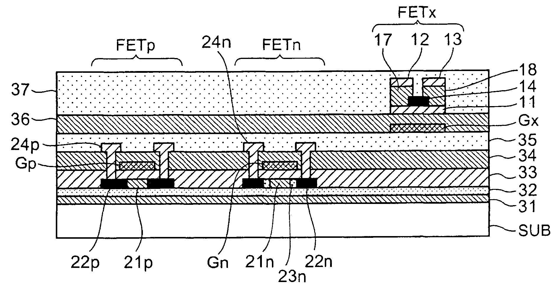
[0060]FIG. 1 is an outline cross-sectional diagram showing the first embodiment of a transistor array element structure related to the present invention.

[0061] Here, FIG. 1 only shows one or several of each field effect transistor (thin-film transistor) using a polysilicon semiconductor layer and an amorphous silicon semiconductor layer in order to simplify explanation. Also, omitted from the drawing is the wiring layer which connects them to one another and the external connection wiring, etc. for connecting with a peripheral device.

[0062] The transistor array element structure related to the first embodiment, as shown in FIG. 1 for example, has a configuration formed in one unit intermingled with P-channel and N-channel types of field effect transistors FETp, FETn (low-temperature polysilicon thin-film transistors) using a semiconduct...

second embodiment

[0097] Next, the transistor array element structure related to the present invention and the second embodiment of its manufacturing method will be explained with reference to the drawings.

[0098] (Element Structure)

[0099]FIG. 5 is an outline cross-sectional diagram showing the second embodiment of the transistor array element structure related to the present invention.

[0100] Here, with respect to any configuration equivalent to the first embodiment (refer to FIG. 1) described above, the equivalent or same nomenclature is appended and further detailed explanation is abbreviated or omitted. Also, FIG. 5 only shows one or several of each field effect transistor (thin-film transistor) using a polysilicon semiconductor layer and an amorphous silicon semiconductor layer in order to simplify explanation. Also, omitted from the drawing is the wiring layer which connects these to one another and the external connection wiring, etc. for connecting a peripheral device.

[0101] In the element ...

third embodiment

[0123] Next, the transistor array element structure related to the present invention and the third embodiment of its manufacturing method will be briefly explained with reference to the drawings.

[0124] (Element Structure)

[0125]FIG. 8 is an outline cross-sectional diagram showing the third embodiment of the transistor array element structure related to the present invention.

[0126] Here, with respect to any configuration equivalent to the first embodiment (refer to FIG. 1) described above, the equivalent or same nomenclature is appended and further detailed explanation is abbreviated or omitted. In addition, FIG. 8 only shows one or several of each field effect transistor using a polysilicon semiconductor layer and photosensor in order to simplify explanation. Also, omitted from the diagram is the wiring layer which connects these to one another and the external connection wiring, etc. for connecting with a peripheral device.

[0127] In the element structure and its manufacturing me...


PUM


Abstract

An image processor by way of a transistor array in which a plurality of transistors are formed on a substrate comprising a plurality of polysilicon thin-film transistors using a first semiconductor layer composed of polysilicon formed on the substrate and functional devices having a plurality of amorphous silicon thin-film transistors using a second semiconductor layer composed of amorphous silicon which are formed in an upper layer more superior than the first semiconductor layer. The polysilicon thin-film transistors and functional devices include a plurality of electrode layers composed of a conductor layer, for instance, the functional devices at least of any one of the electrode layers are formed in the same layer as any one the electrode layers of the polysilicon thin-film transistors.

Description

CROSS-REFERENCE TO RELATED APPLICATIONS [0001] This application is based upon and claims the benefit of priority from the prior Japanese Patent Applications No. 2004-020968, filed Jan. 29, 2004; No. 2004-035622, filed Feb. 12, 2004; and No. 2004-039371, filed Feb. 17, 2004, the entire contents of which is incorporated herein by reference. BACKGROUND OF THE INVENTION [0002] 1. Field of the Invention [0003] The present invention relates to a transistor array, the manufacturing method thereof and an image processor which uses the same. More particularly, the present invention relates to the element structure of a transistor array configuration comprising polysilicon thin-film transistors and amorphous silicon thin-film transistors, the associated manufacturing method and an image processor that applies the aforesaid transistor array. [0004] 2. Description of the Related Art [0005] Recently, Research and Development (R&D) has become more highly advanced for applying personal authenticat...

Claims


Application Information

Patent Timeline
IPC IPC(8): H01L21/00G02F1/136H01L21/77H01L21/822H01L21/84H01L27/00H01L27/06H01L27/12H01L31/10H04N1/00
CPCH01L21/8221H01L29/78621H01L27/1251H01L27/0688G02F1/136
Inventor SASAKI, KAZUHIROMATSUMOTO, HIROSHISUMI, SHINOBU
Owner BOE TECH GRP CO LTD
Why Eureka
Try Eureka