Plasma display panel

a display panel and plasma technology, applied in the direction of discharge tube main electrodes, identification means, instruments, etc., can solve the problems of reducing the afterimage time, generating afterimages, and not being able to meet the requirements of hdtv, so as to reduce the afterimage time, reduce the hardness, and the effect of light weigh

Inactive Publication Date: 2005-08-18
LG ELECTRONICS INC
View PDF11 Cites 9 Cited by
  • Summary
  • Abstract
  • Description
  • Claims
  • Application Information

AI Technical Summary

Benefits of technology

[0020] The present invention is advantageous in that it can reduce an afterimage time. Further, according to the present invention, a sheet of a low hardnes

Problems solved by technology

However, a display device, which is satisfactory to HDTV, has not yet been completed in terms of technology.
However, this PDP has a problem in that afterimage is gener

Method used


Image

  • Plasma display panel
  • Plasma display panel
  • Plasma display panel

Examples


first embodiment

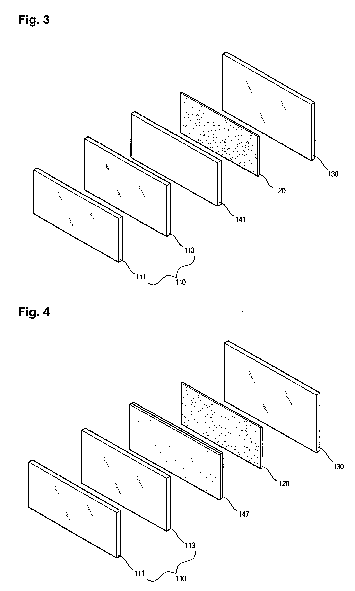
[0060]FIG. 3 is a dismantled perspective view illustrating the construction a PDP according to the present invention.

[0061] Referring to FIG. 3, the PDP according to the present invention includes a panel unit 110 having an upper plate 111 and a lower plate 113, a metal layer 141 laminated on a bottom surface of the lower plate 113 of the panel unit 110, a sheet 120 formed on a bottom surface of the metal layer 141, and a frame 130 disposed opposite to the panel unit 110 with the metal layer 141 and the sheet 120 located therebetween.

[0062] The metal layer 141 can be formed on the bottom surface of the lower plate 113 by coating a conductive paste on a glass substrate of the lower plate 113 or coating a metal on the glass substrate of the lower plate 113 by means of a sputtering method, etc. The metal layer 141 is formed on the lower plate 113 in a floating state. The metal layer 141 has influence upon charges, which are introduced into the lower plate 113, to improve the waveform ...

second embodiment

[0065]FIG. 4 is a dismantled perspective view illustrating the construction a PDP according to the present invention.

[0066] Referring to FIG. 4, the PDP according to the present invention includes a panel unit 110 having an upper plate 111 and a lower plate 113, a metal tape 147 adhered to a bottom surface of the lower plate 113 of the panel unit 110, a sheet 120 attached to a bottom surface of the metal tape 147, and a frame 130 adhered to the panel unit 110 through the sheet 120, wherein the frame 130 radiates heat transferred through the sheet 120.

[0067] It is preferred that the metal tape 147 has an adhesive at least on one side for the purpose of adhesion with the panel unit 110 and / or the sheet 120, and the adhesive has conductivity. The metal tape 147 can be attached to the lower plate 113 in a floating state, or can be grounded to a ground voltage (GND).

third embodiment

[0068]FIG. 5 is a dismantled perspective view illustrating the construction a PDP according to the present invention.

[0069] Referring to FIG. 5, the PDP according to the present invention includes a panel unit 110 having an upper plate 111 and a lower plate 113, a metal sheet 143 laminated on a bottom surface of the lower plate 113 of the panel unit 110, an insulating sheet 145 laminated on a bottom surface of the metal sheet 143, a sheet 120 attached to a bottom surface of the insulating sheet 145, and a frame 130 adhered to the panel unit 110 through the sheet 120, wherein the frame 130 radiates heat transferred through the sheet 120.

[0070] The metal sheet 143 and the insulating sheet 145 can be used with them melted / compressed into one. The metal sheet 143 has influence upon remaining charges that are introduced into the lower plate 113. The metal sheet 143 can be attached to the lower plate 113 in a floating state, or can be grounded to a ground voltage (GND).

[0071] The insula...


PUM


Abstract

Disclosed herein is a plasma display panel in which afterimage is improved. The plasma display panel according to the present invention includes a panel unit having an upper plate and a lower plate, a frame that supports circuitry, and a conductive material formed between the panel unit and the frame. As such, a conductive material is formed on a bottom surface of a lower plate of a panel. Thus, charges introduced into the lower plate are properly controlled to improve the waveform stability of the panel. Also, a charge characteristic is improved to implement a stable operation. Accordingly, an afterimage time can be reduced. Further, a sheet of a low hardness and light weight is used. It is thus possible to absorb shock and noise of a PDP, accomplish light weight of the PDP and reduce the materials of the sheet.

Description

[0001] This Nonprovisional application claims priority under 35 U.S.C. §119(a) on Patent Application No. 10-2004-0003208 filed in Korea on Jan. 16, 2004, Patent Application No. 10-2004-0082728 filed in Korea on Oct. 15, 2004, the entire contents of which are hereby incorporated by reference. BACKGROUND OF THE INVENTION [0002] 1. Field of the Invention [0003] The present invention relates to a plasma display panel. More particularly, the present invention relates to a plasma display panel in which afterimage is reduced, wherein a conductive material is formed on a bottom surface of a lower plate of the panel to properly control charges introduced into the lower plate, whereby waveform stability of the panel and a charge characteristic are improved to implement a stable operation. Further, the present invention relates to a plasma display panel, which is adapted to absorb shock and noise and also suitable for light weight [0004] 2. Description of the Background Art [0005] Recently, th...

Claims


Application Information

Patent Timeline
IPC IPC(8): G09F9/00H01J11/12H01J11/34H01J17/49
CPCH01J11/34H01J11/12
Inventor KIM, DEOK SOOLEE, BYUNG CHULKIM, JIN YOUNGKIM, YUN GISHIN, SUNG GONJUN, SUNG MIN
Owner LG ELECTRONICS INC
Why Eureka
Try Eureka