Dislay element and display device

Active Publication Date: 2005-08-18
SHARP KK
View PDF10 Cites 100 Cited by
  • Summary
  • Abstract
  • Description
  • Claims
  • Application Information

AI Technical Summary

Benefits of technology

[0023] As described above, in the conventional liquid crystal display element, the display operation is carried out by utilizing only the change in the orientational direction of the liquid crystal molecules due to rotation thereof caused by the electric field application. The liquid crystal molecules in alignment are rotated together in one direction. Thus, inherent viscosity of the liquid crystal largely affects responding speed. On the other hand, the present invention, in which the display is carried out by utilizing the change in the modulation of the optical anisotropy in the medium, is free from the problem that the inherent viscosity of the liquid crystal largely affects responding speed, unlike the conventional liquid crystal display element. Thus, it is possible to realize high-speed responding. Moreover, the high-speed responding allows the display element to be used, for example, in a display device of the field sequential color mode.
[0024] Moreover, the conventional liquid crystal display element has such a problem that its driving temperature range is limited to temperatures near a phase transition point of a liquid crystal phase, and thus it requires a highly accurate temperature control. On the other hand, the present invention is only required that the medium be kept at temperatures at which the magnitude of the optical anisotropy is changeable by the application of the electric field. Thus, it is possible to easily perform the temperature control in the preset invention.
[0025] Moreover, according to the present invention, it is possible to realize a wider viewing angle property than in the conventional liquid crystal display element, because the present invention utilizes, for performing the display operation, the change in the magnitude of the optical anisotropy of the medium, whereas the conventional liquid crystal display element utilizes, for performing the display operation, the change in the

Problems solved by technology

However, the liquid crystal display elements using the TN mode have disadvantages such as slow response, narrow viewing angle, and similar drawbacks.
Those disadvantages are large hindrances for the TN mode to take over CRT (Cathode Ray Tube).
Moreover, the display mode in which FLC or AFLC is used has advantages such as high-speed response and wide viewing angles, but is significantly poor in shock-resistant property and temperature property.
Therefore, the display mode in which the FLC or AFLC is used has not been widely in practical use.
However, in principle, the polymer dispersion type liquid crystal dis

Method used


Image

  • Dislay element and display device
  • Dislay element and display device
  • Dislay element and display device

Examples


embodiment 1

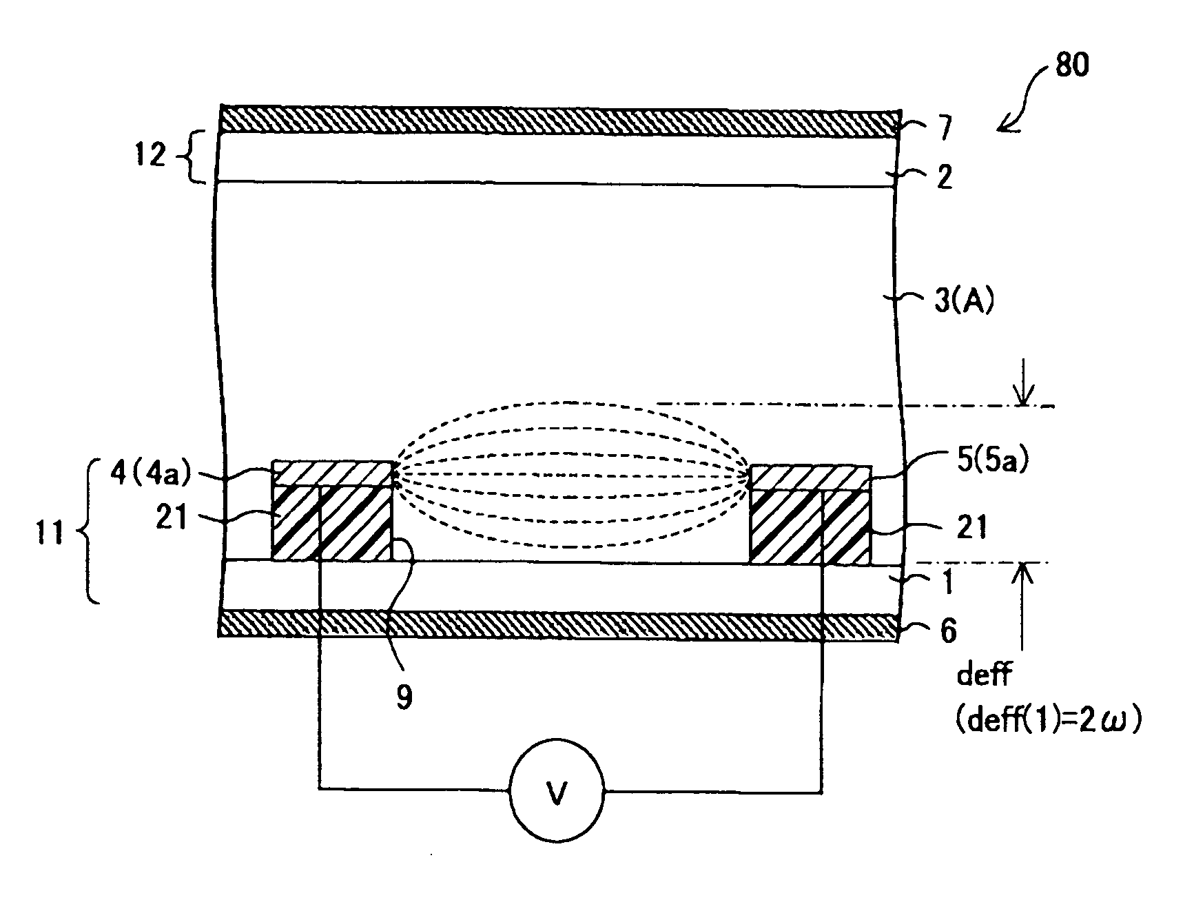
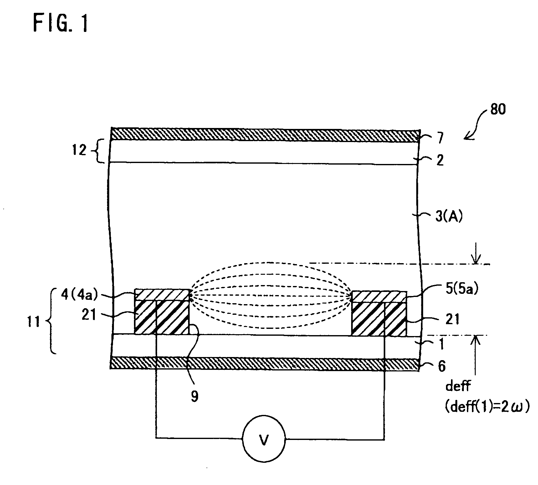
[0067] The following description explains one embodiment of the present invention in reference to FIGS. 1 to 14 and FIGS. 22 to 24.

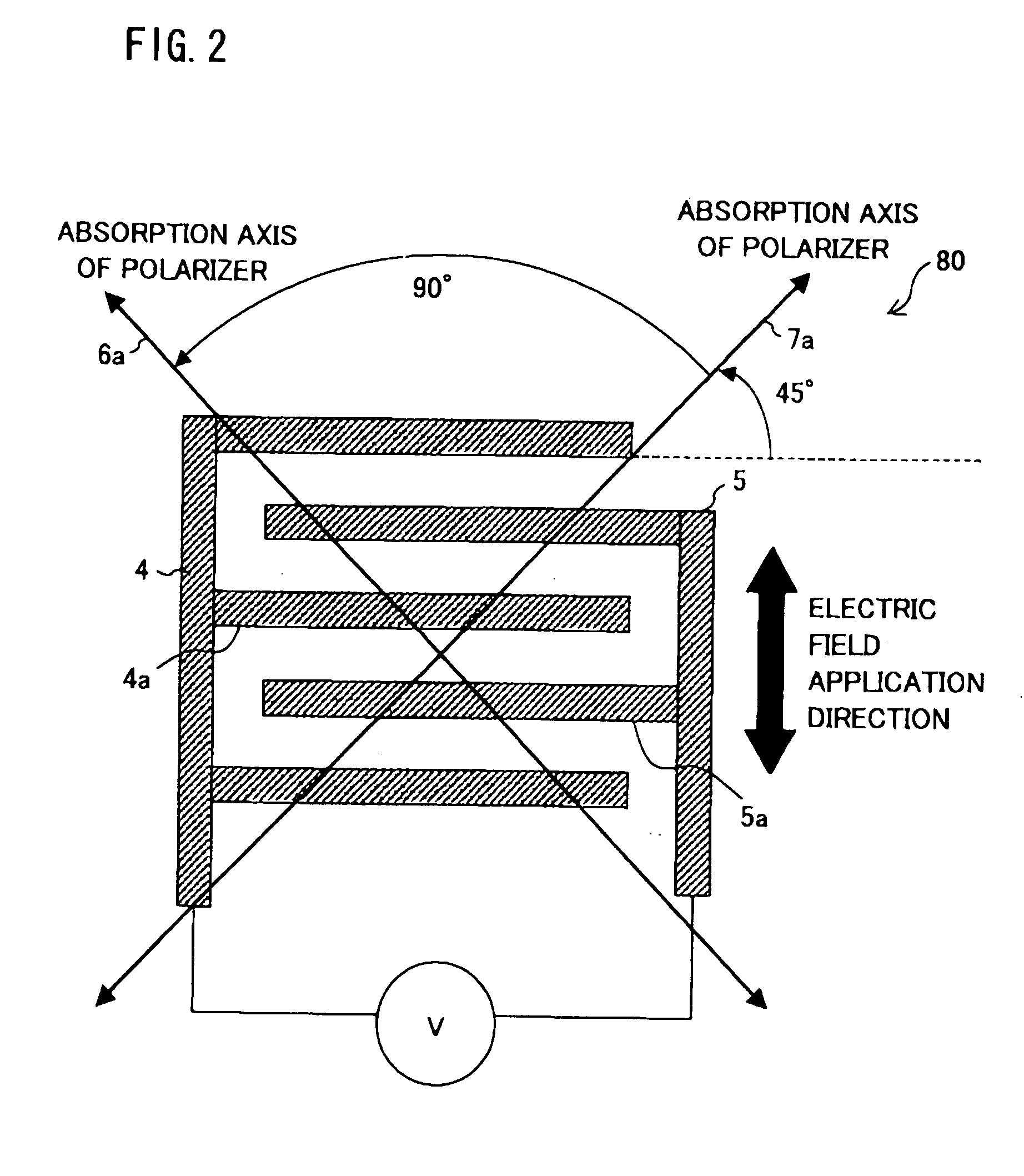
[0068]FIG. 1 is a cross-sectional view illustrating a schematic arrangement of substantial parts of a display element in accordance with the present embodiment. FIG. 2 is a view for explaining a relationship between an electrode structure and polarizing plate absorption axes in the display element. FIG. 22 is a block diagram illustrating a schematic arrangement of substantial parts of a display device using the display element in accordance with the present invention. FIG. 23 is a schematic diagram illustrating a schematic arrangement around the display element used in the display device illustrated in FIG. 22.

[0069] The display element in accordance with the present embodiment is provided in the display device together with a drive circuit, signal lines (data signal lines), scanning lines (scanning signal lines), switching elements, etc.

[0070] As ill...

embodiment 2

[0203] The following description explains another embodiment of the present invention in reference to FIGS. 15 and 16. Note that, the present embodiment mainly explains points different from points described in Embodiment 1. The same reference numerals are used for the members having the same functions as the members used in Embodiment 1, and further explanations thereof are omitted.

[0204] Embodiment 1 explained a case where each of the comb-shaped electrodes 4 and 5 is stacked above the substrate 1 via the insulating layer 21 which is formed (patterned) in a comb-like shape, which is just like the shape of each of the comb-shaped electrodes 4 and 5. The present embodiment explains a case where a plurality of the comb-shaped electrodes 4 are formed via the insulating layers 21 and a plurality of the comb-shaped electrodes 5 are formed via the insulating layers 21.

[0205] That is, the display element 80 of the present embodiment is structured such that a pair of substrates 1 and 2 a...

embodiment 3

[0216] The following description explains yet another embodiment of the present invention in reference to FIGS. 17 to 19. Note that, the present embodiment mainly explains points different from points described in Embodiments 1 and 2. The same reference numerals are used for the members having the same functions as the members used in Embodiments 1 and 2, and further explanations thereof are omitted.

[0217] Each of FIGS. 17 to 19 is a cross-sectional view illustrating an example of a schematic arrangement of substantial parts of the display element in accordance with the present embodiment.

[0218] Embodiments 1 and 2 explained a case where each of the comb-shaped electrodes 4 and 5 are stacked on and above the substrate 1 via the insulating layer 21 which is formed (patterned) in a comb-like shape, which is just like the shape of each of the comb-shaped electrodes 4 and 5. The present embodiment explains a case where the thickness of the comb-shaped electrodes 4 and 5 are increased ...


PUM


Abstract

A display element of the present invention includes: a pair of substrates at least one of which is transparent; a medium layer, made of a medium sandwiched between the substrates 1 and 2, whose magnitude of an optical anisotropy is changed by applying an electric field; and at least a pair of electrodes applying to the medium layer an electric field which is substantially parallel to the substrates. The electrodes are provided above the substrate via insulating layers each of which is formed in a convex shape. Therefore, a maximal electric field region generated by the electrodes is separated from interfaces of the substrates.

Description

[0001] This Nonprovisional application claims priority under 35 U.S.C. § 119(a) on Patent Application Nos. 2004 / 9832 and 2005 / 6872 filed in Japan respectively on Jan. 16, 2004 and on Jan. 13, 2005, the entire contents of which are hereby incorporated by reference. FIELD OF THE INVENTION [0002] The present invention relates to a display element and a display device each of which has a high-speed response property and a wide viewing angle display property. BACKGROUND OF THE INVENTION [0003] As compared with various display elements, a liquid crystal display element has advantages such as thinner size, light weight, and lower power consumption. The liquid crystal display element is widely used in image display apparatuses such as televisions, videocassette recorders, and the like, and OA (Office Automation) apparatuses such as monitors, word processors, personal computers, and the like. [0004] Conventionally known liquid crystal display methods of the liquid crystal display elements ar...

Claims


Application Information

Patent Timeline
IPC IPC(8): C09K19/02G02F1/133G02F1/1343
CPCC09K19/02G02F1/134363C09K2019/0418
Inventor MIYACHI, KOICHISHIBAHARA, SEIJIINOUE, IICHIROJINDA, AKIHITOKOIDE, TAKAKOOGISHIMA, KIYOSHI
Owner SHARP KK
Why Eureka
Try Eureka